


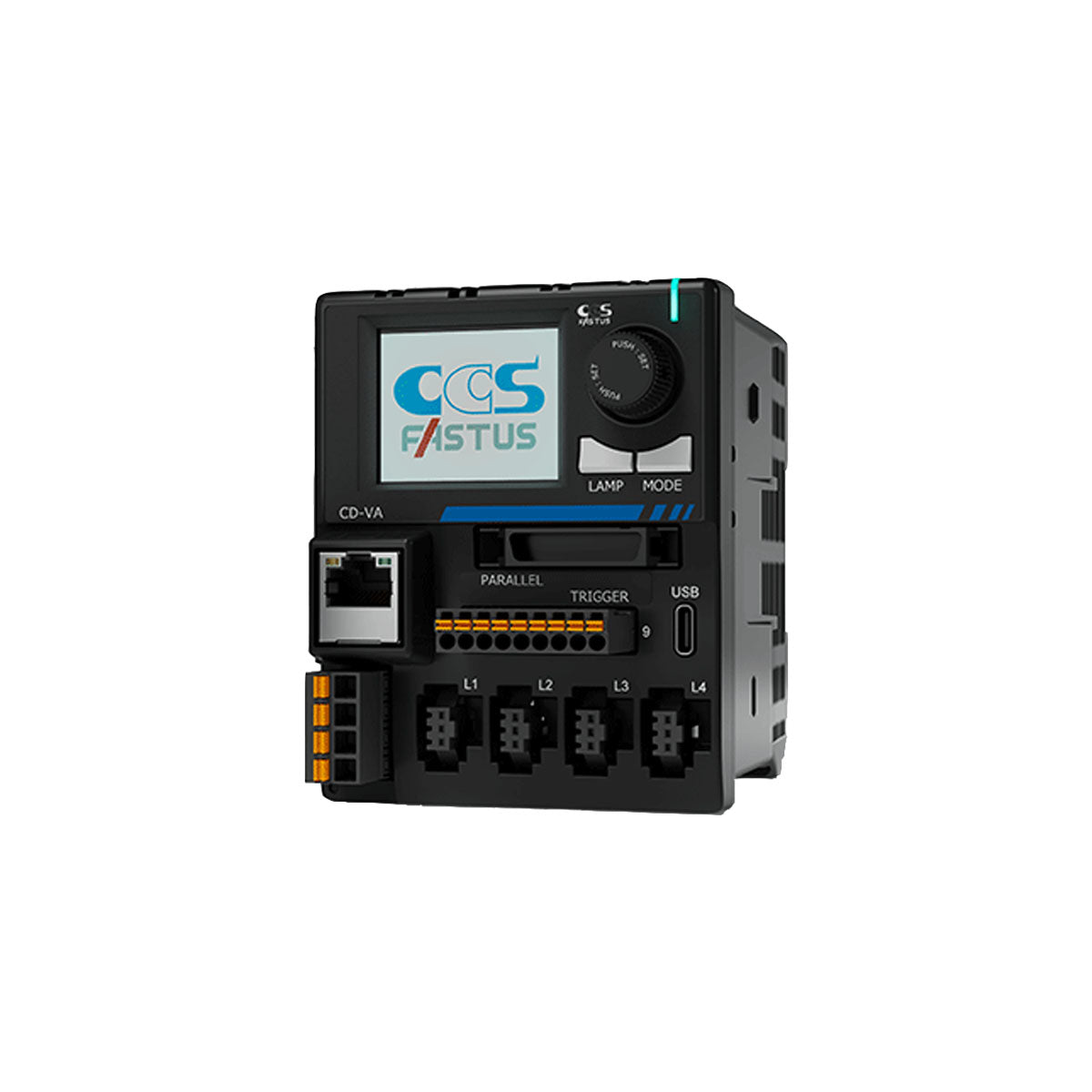
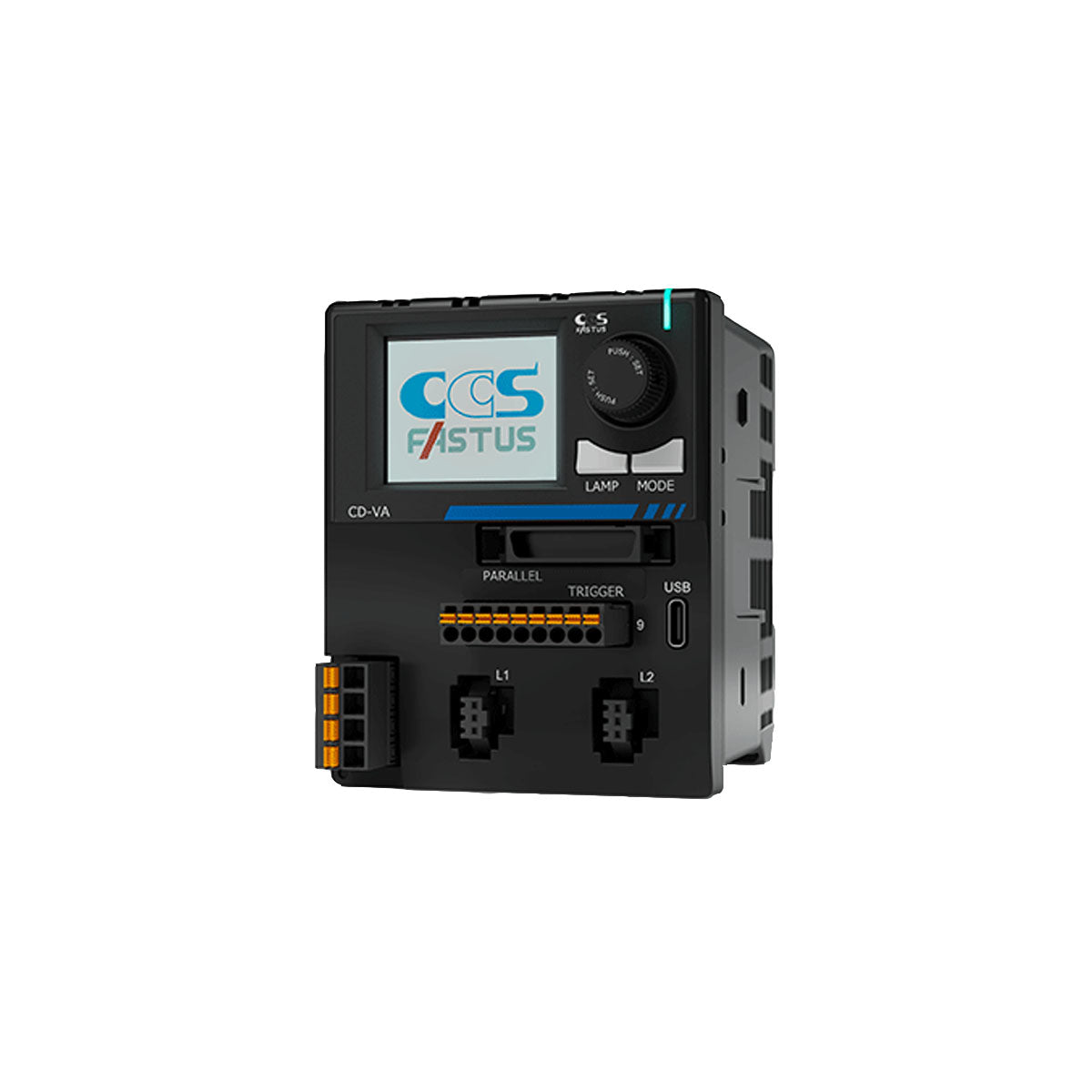


 Lighting


The semiconductor industry continues to push the boundaries of precision manufacturing. As device geometries shrink and production volumes increase, inspection systems must identify smaller defects, operate at higher speeds and maintain exceptional image quality throughout the manufacturing process.
At the heart of these inspection systems is the machine vision camera. Whether inspecting wafers, semiconductor packages, PCBs or microelectronic components, selecting the right camera can significantly impact yield, throughput, and quality control.
The Growing Challenges of Semiconductor Inspection
Modern semiconductor manufacturing requires imaging systems capable of detecting microscopic defects that could affect device performance. These defects may include:
- Surface contamination
- Scratches and cracks
- Pattern defects
- Alignment errors
- Bonding defects
- Foreign particles
- Edge chipping
To identify these issues reliably, machine vision systems must excel in three critical areas: resolution, cleanliness and speed.
High Resolution for Microscopic Defect Detection
As semiconductor sizes continue to decrease, inspection systems require increasingly higher resolutions to maintain accurate defect detection.
High-resolution machine vision cameras allow manufacturers to:
- Capture fine details across large wafers
- Detect sub-micron defects
- Reduce false positives and false rejects
- Improve process monitoring and traceability
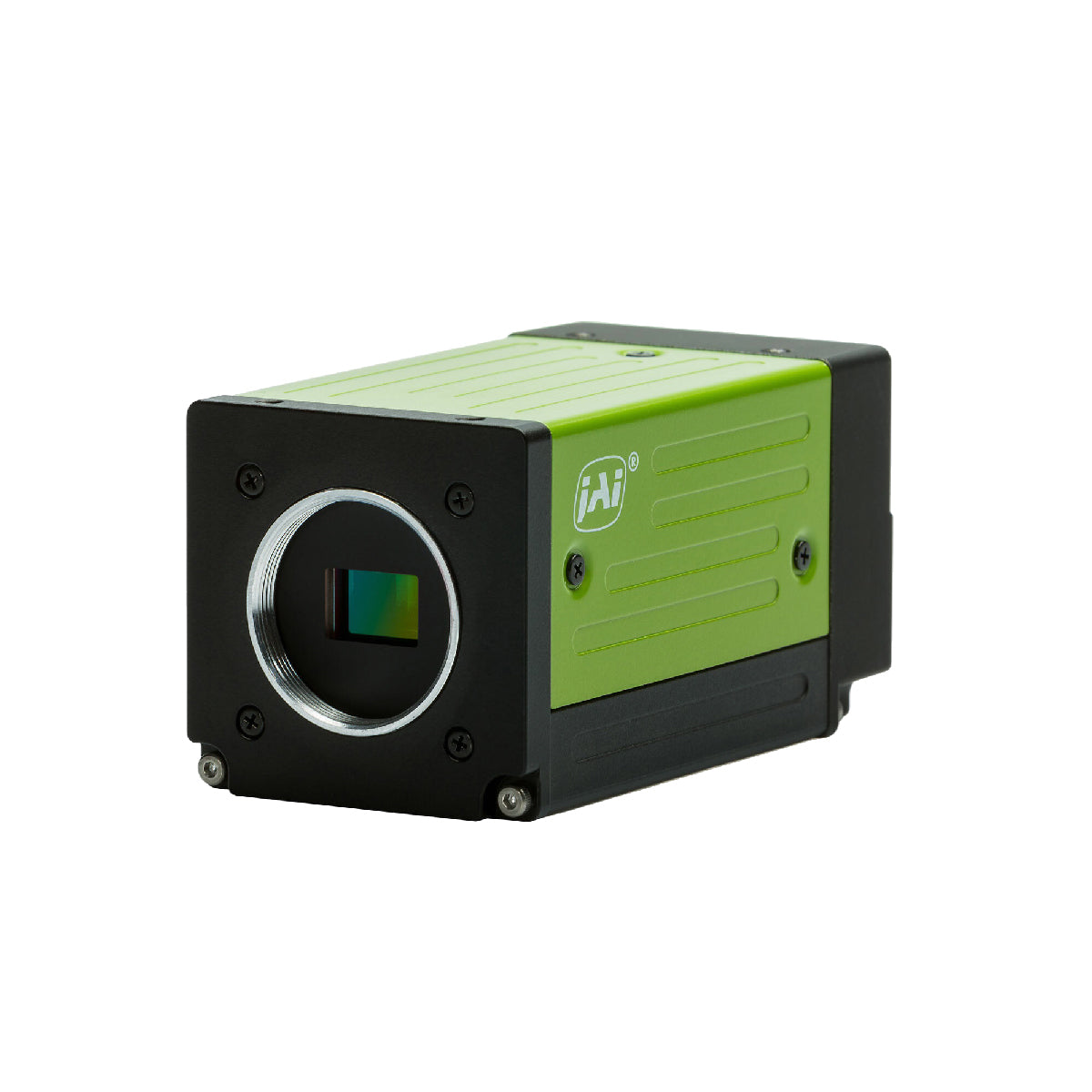
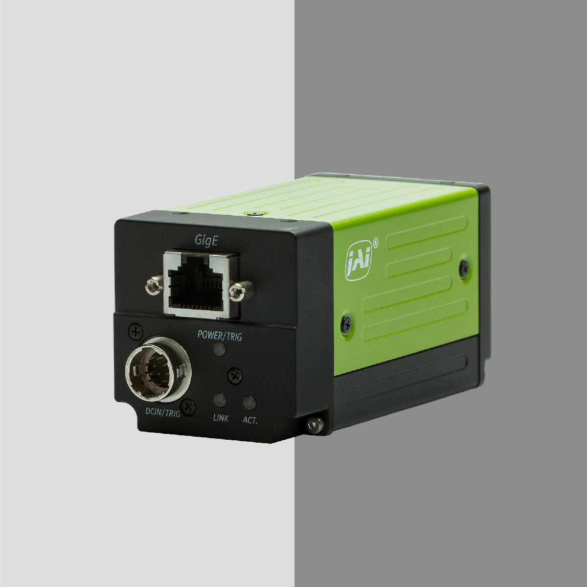
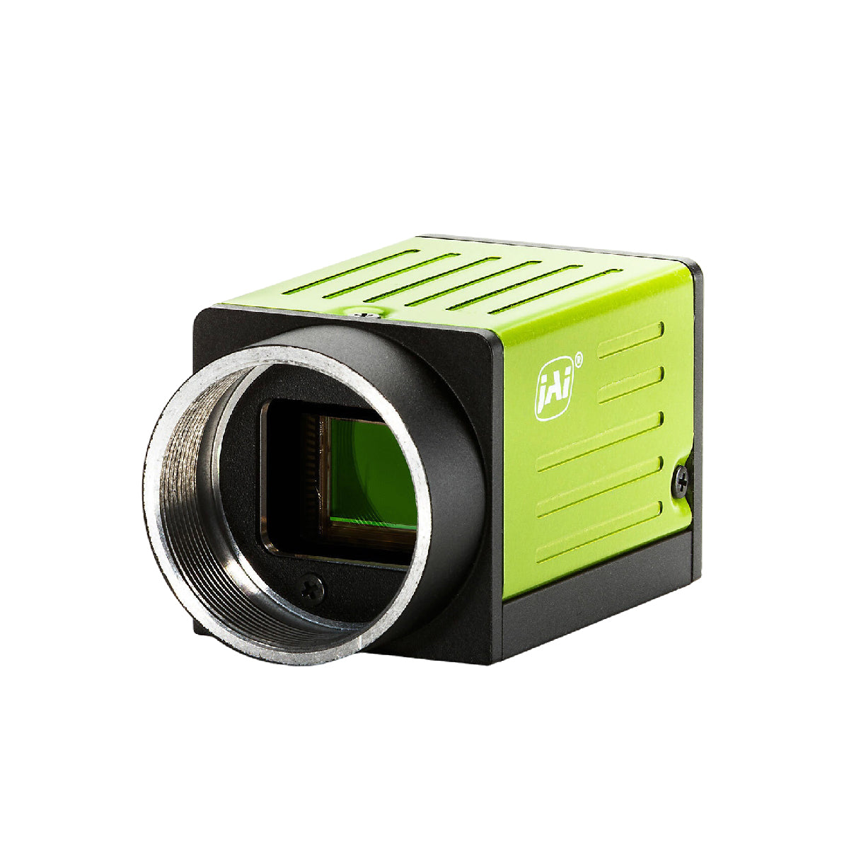
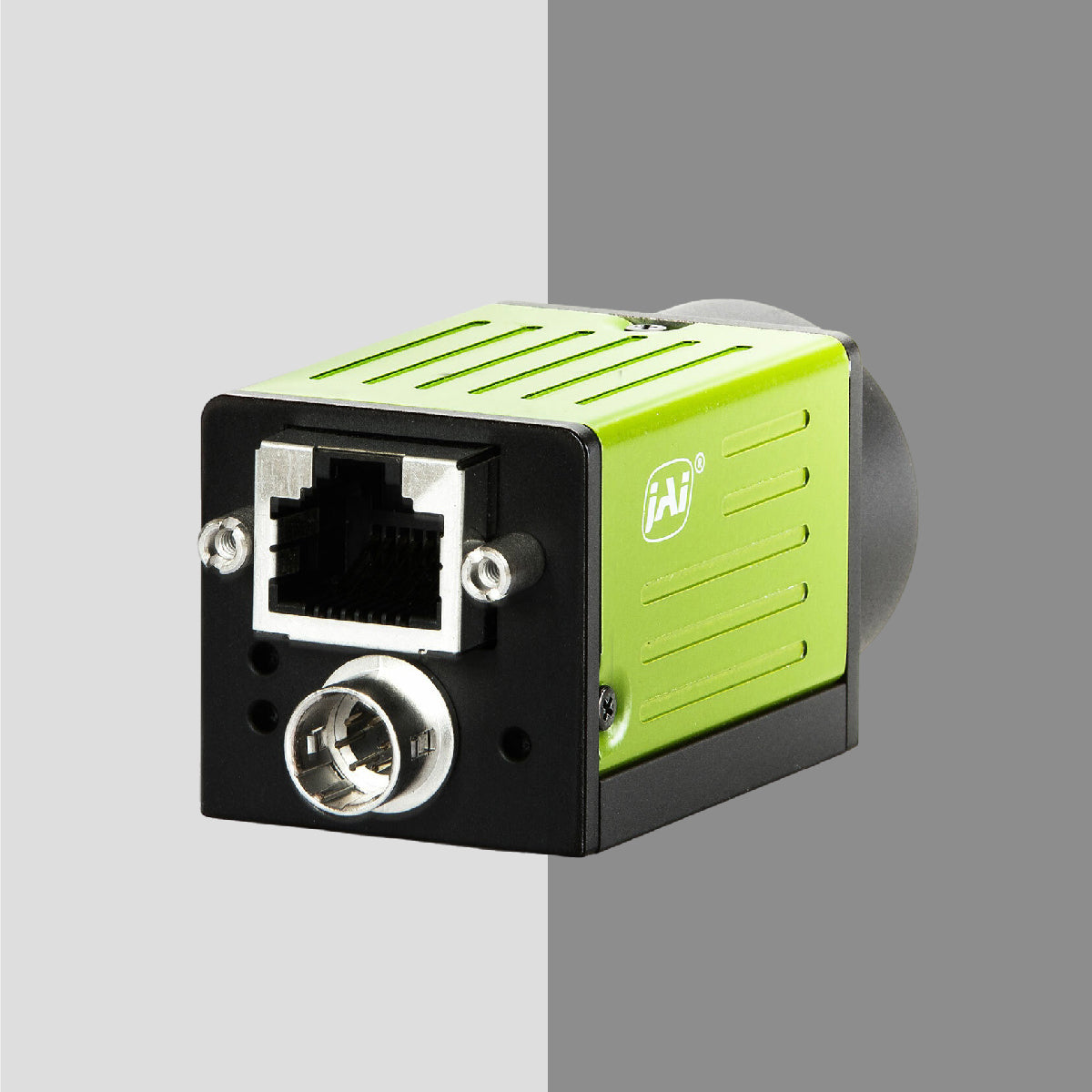
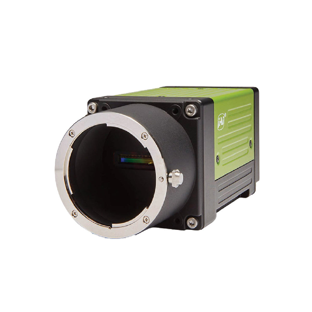
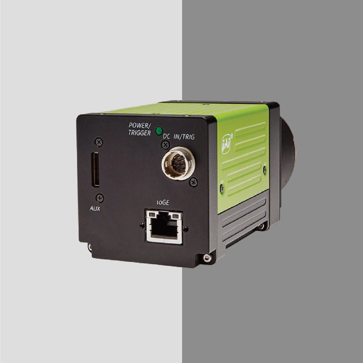
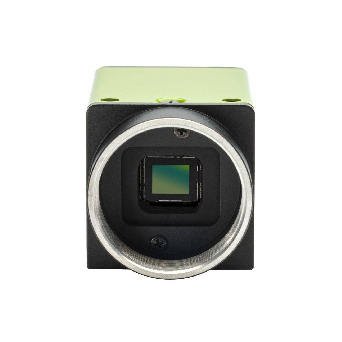
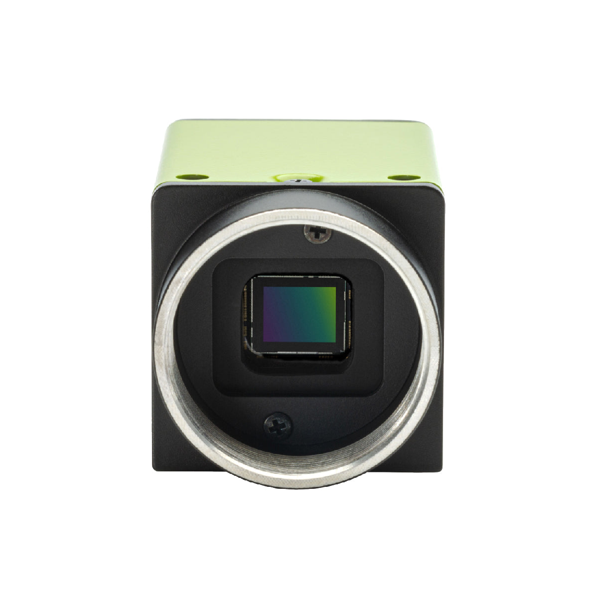
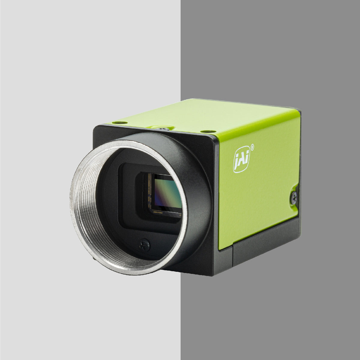
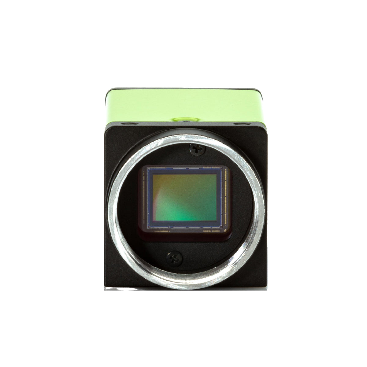
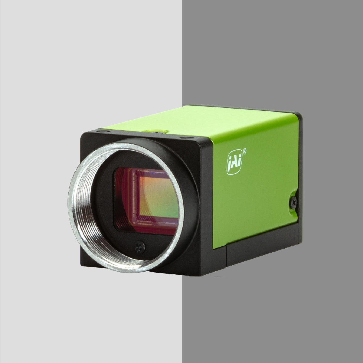
FJW high-performance area scan cameras are designed to meet these requirements. Cameras such as the Go-X Series provide resolutions exceeding 20 megapixels while maintaining excellent image quality and low noise performance.
For wafer inspection applications, high-resolution sensors allow larger fields of view while preserving the pixel density needed to identify extremely small imperfections. This reduces the number of images required to inspect a wafer, helping improve overall system efficiency.
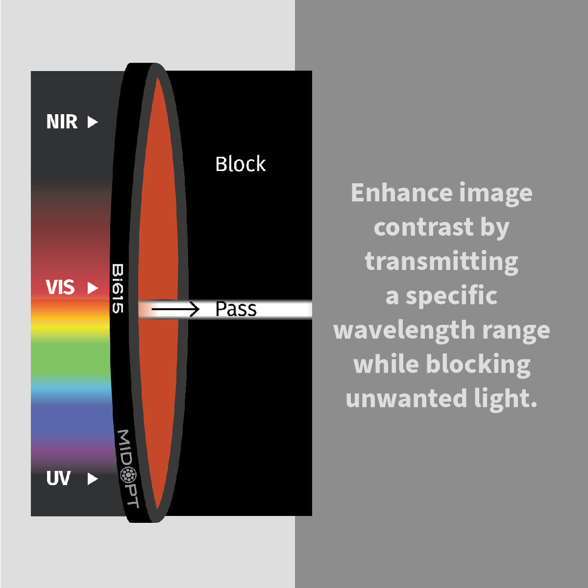
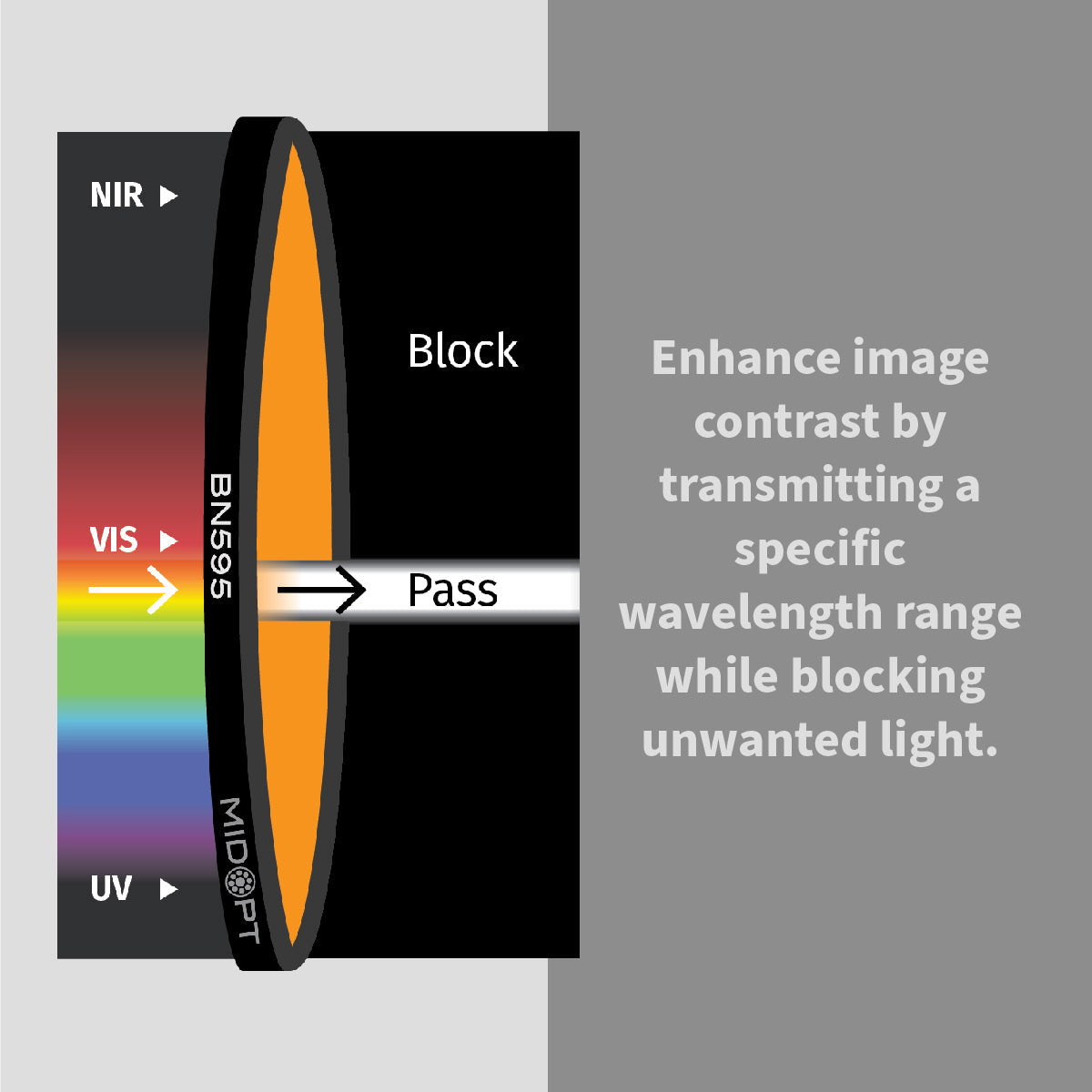
Maintaining Image Cleanliness
In semiconductor inspection, image quality extends beyond resolution alone.
Even the highest-resolution sensor cannot compensate for poor image contrast, excessive noise or inconsistent illumination. Inspection systems must produce clean, repeatable images that allow software algorithms to accurately identify defects and process variations.
Key camera features that contribute to image cleanliness include:
Low Noise Performance
Advanced sensor architectures minimize image noise, allowing subtle defects and low-contrast features to become more visible.
High Dynamic Range
Wafer surfaces often contain highly reflective regions alongside darker materials. Cameras with strong dynamic range capabilities help maintain detail across varying brightness levels without overexposure.
Precise Color Reproduction
Certain semiconductor and electronics inspection applications benefit from accurate color imaging to differentiate materials, coatings and process conditions.
Prism-based multi-sensor color cameras capture true RGB data simultaneously, eliminating interpolation artifacts common with Bayer-pattern sensors and providing exceptional color fidelity for demanding inspection tasks.
High-Speed Inspection for Maximum Throughput
Semiconductor fabs operate around the clock, making throughput a critical performance metric.
Inspection systems must keep pace with automated production lines without sacrificing image quality. High-speed imaging reduces bottlenecks and helps maximize equipment utilization.
Modern machine vision cameras offer several advantages for high-throughput inspection:
Fast Frame Rates
High-speed area scan cameras capture more images per second, allowing wafers and components to move through inspection stations more quickly.
High-Bandwidth Interfaces
GigE Vision, 5GigE, 10GigE and CoaXPress interfaces enable rapid image transfer from the camera to the processing system, reducing latency and improving overall inspection efficiency.
Line Scan Solutions
For continuous wafer transport and web-based inspection processes, line scan cameras provide exceptional resolution while maintaining high inspection speeds.
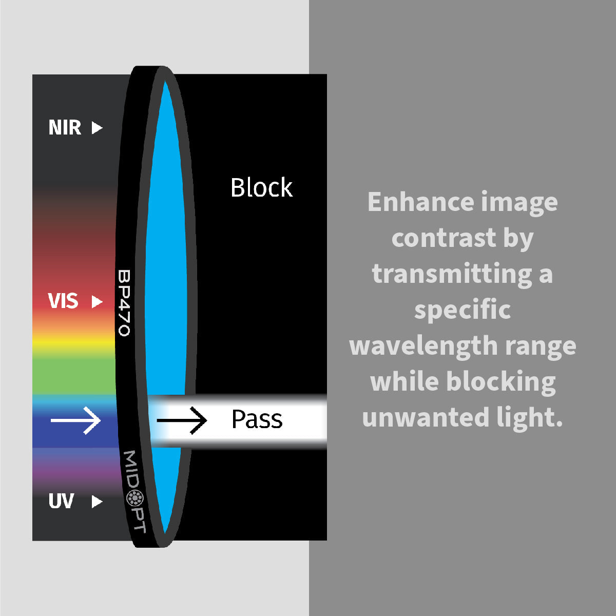
Multispectral Imaging for Advanced Defect Detection
As semiconductor devices become more complex, traditional visible-light inspection may not reveal every defect.
Multispectral imaging combines visible (VIS) and near-infrared (NIR) imaging capabilities to uncover features hidden beneath surface layers or identify material variations that would otherwise go undetected.
By simultaneously capturing VIS and NIR images using a single optical path, it simplifies system design while expanding inspection capabilities.
This technology can help identify:
- Material inconsistencies
- Surface contamination
- Coating defects
- Bonding irregularities
- Process anomalies
Building a Complete Semiconductor Vision System
While cameras are the foundation of any inspection system, optimal results require the right combination of:
- High-resolution machine vision cameras
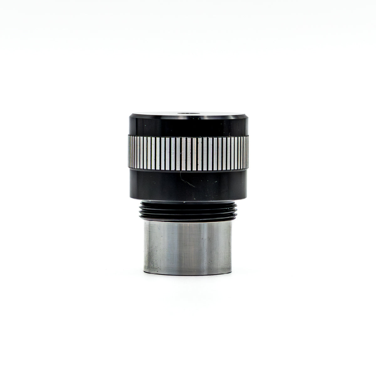
- Precision machine vision lenses
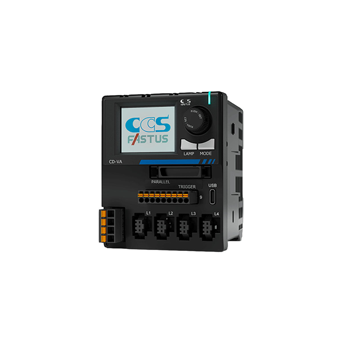
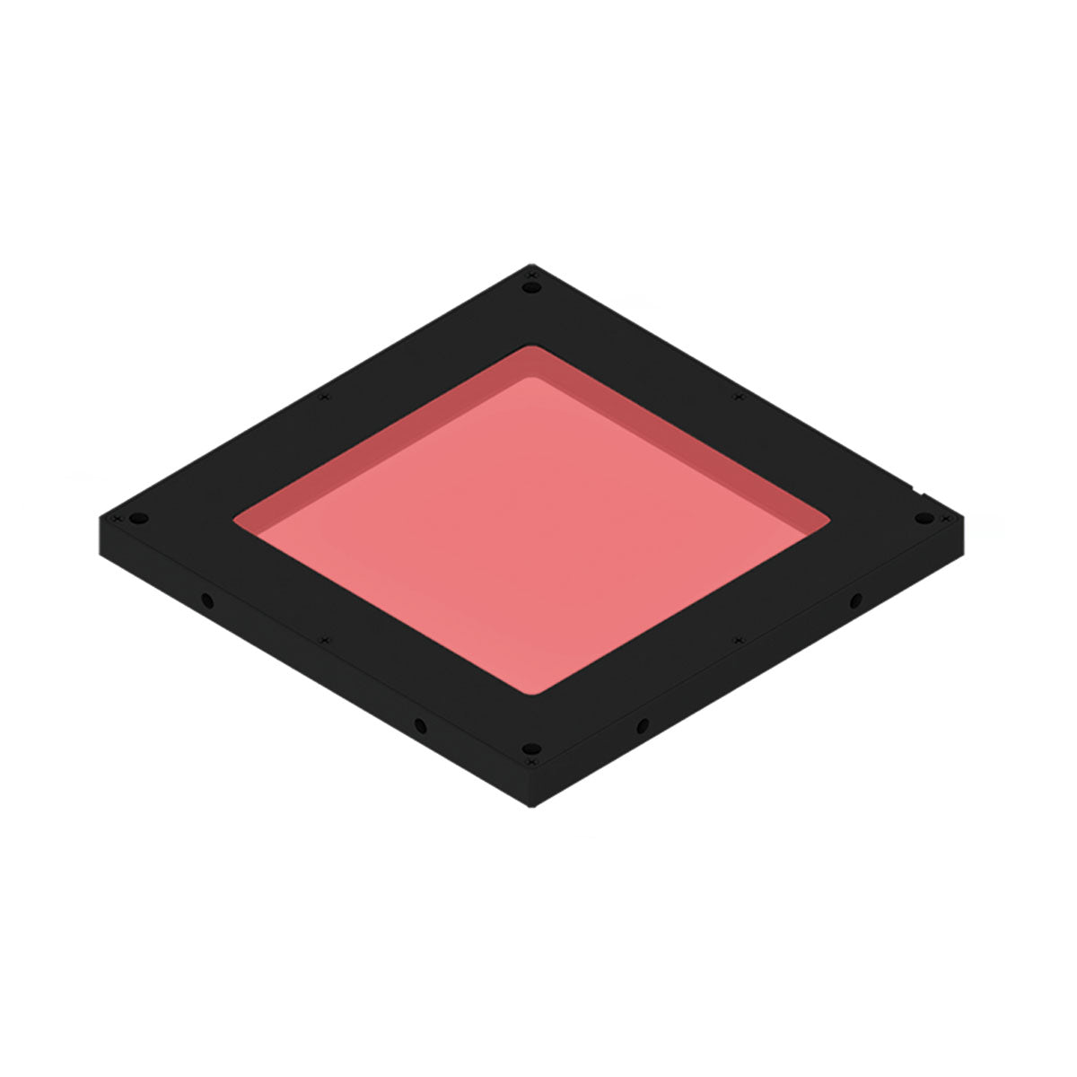
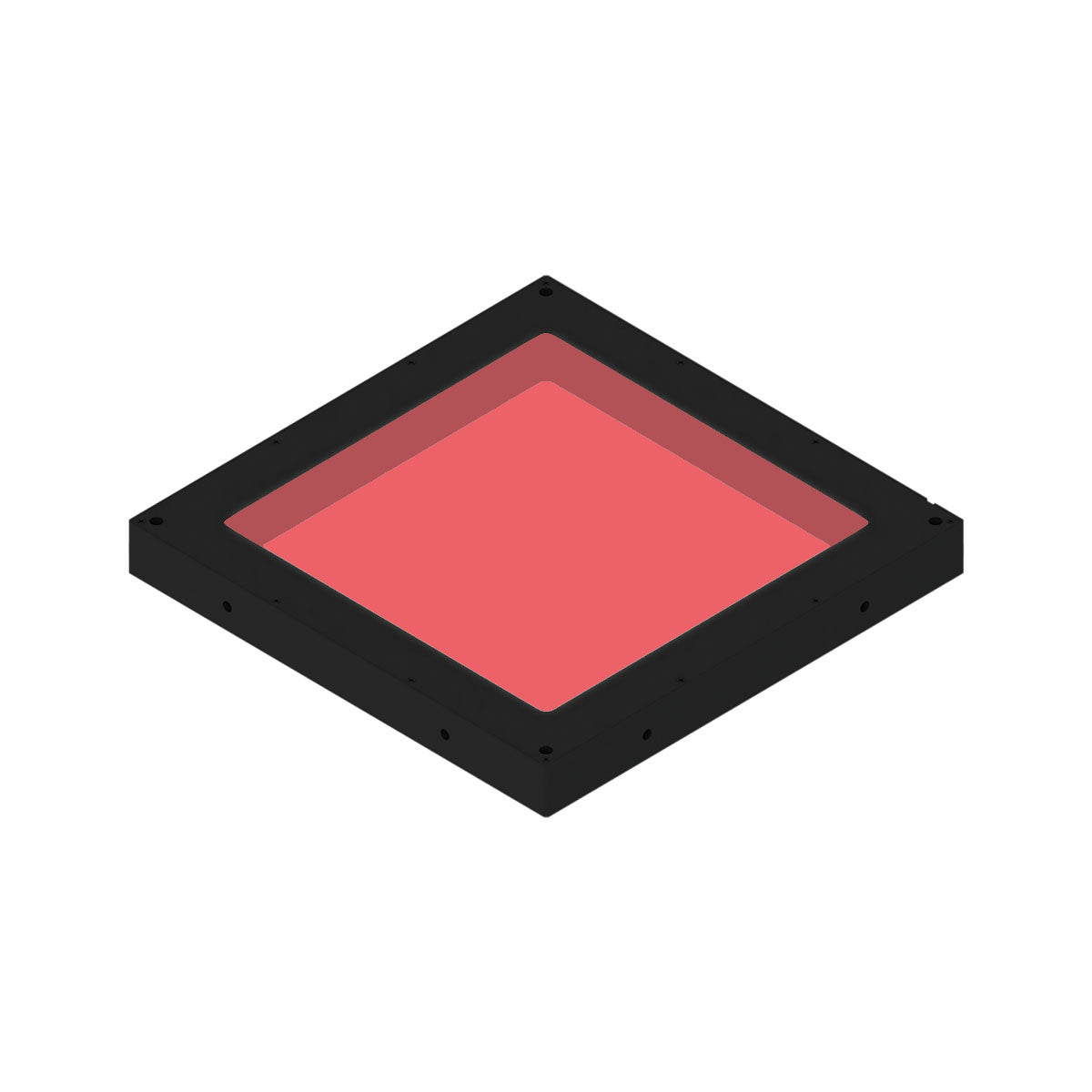
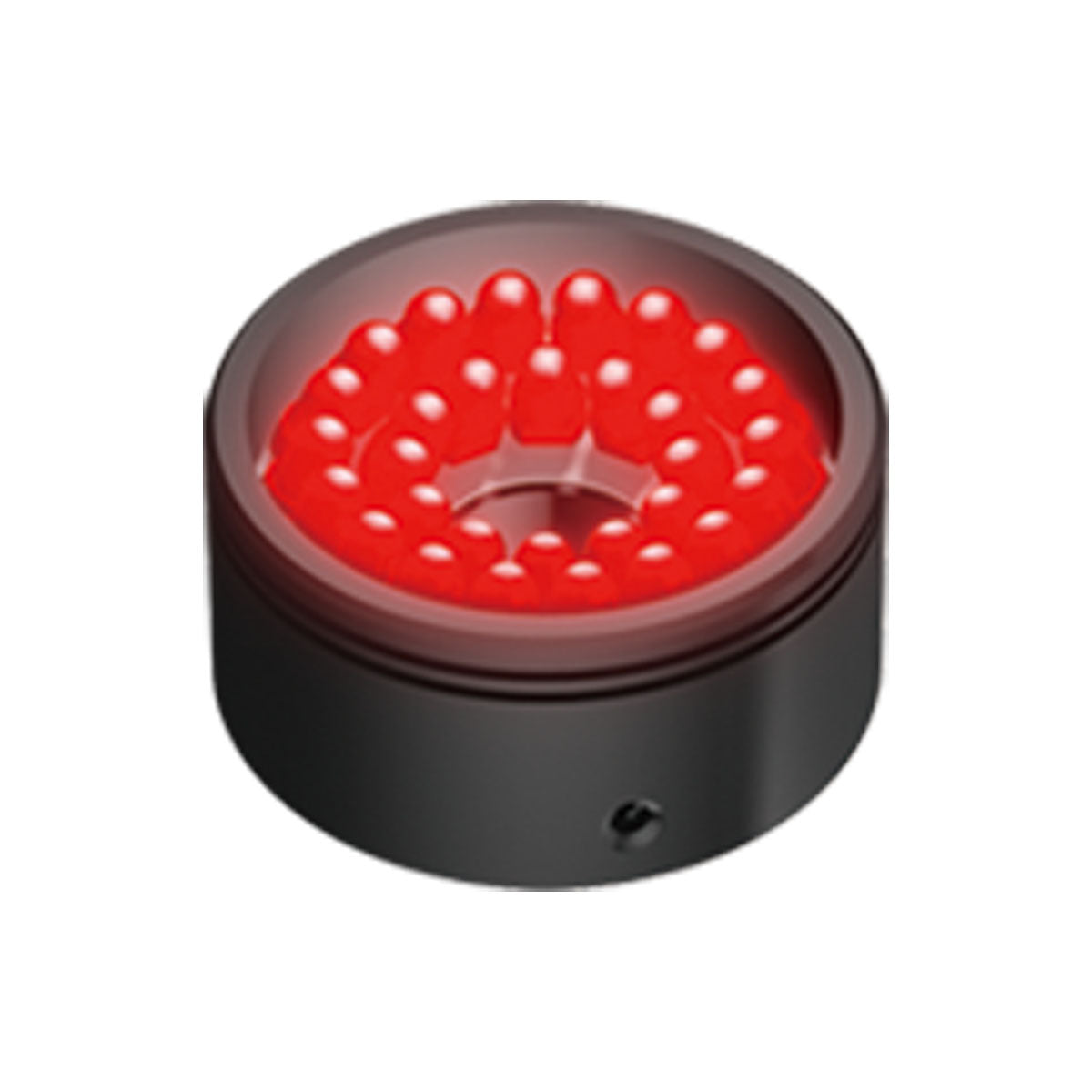
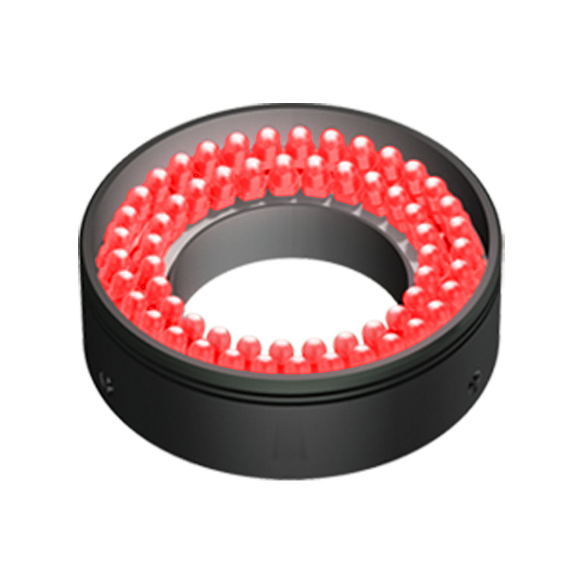
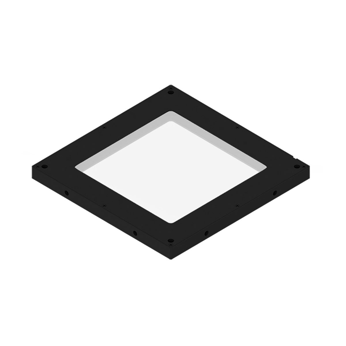
- Specialized LED illumination
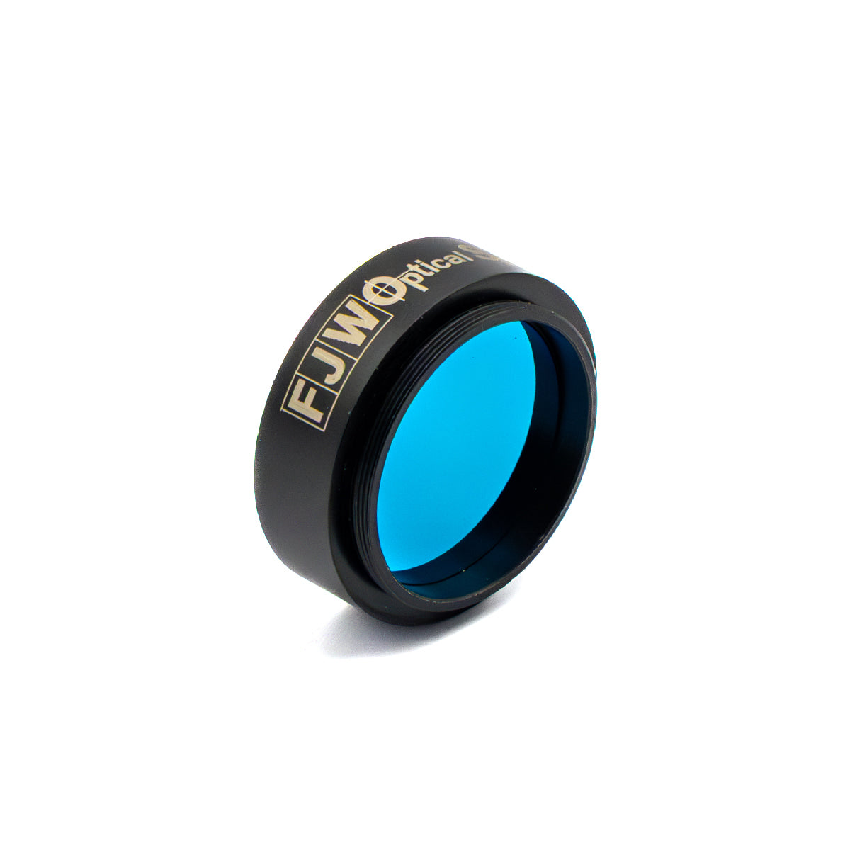
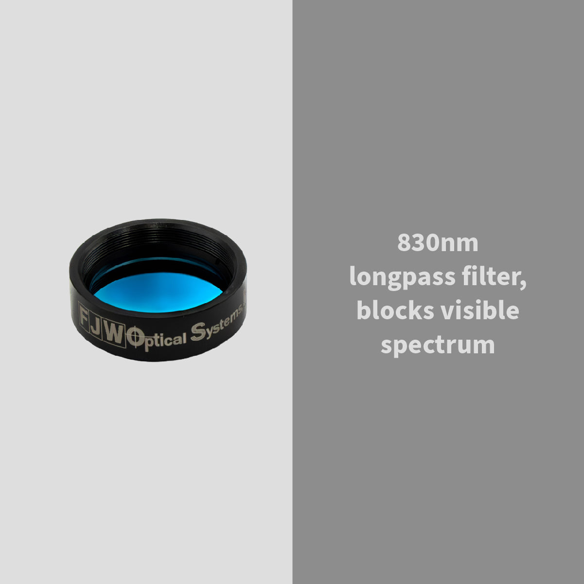
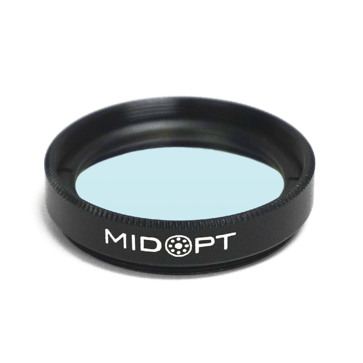
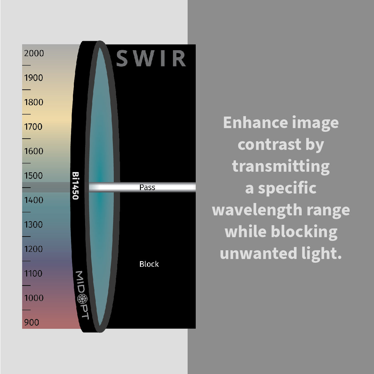
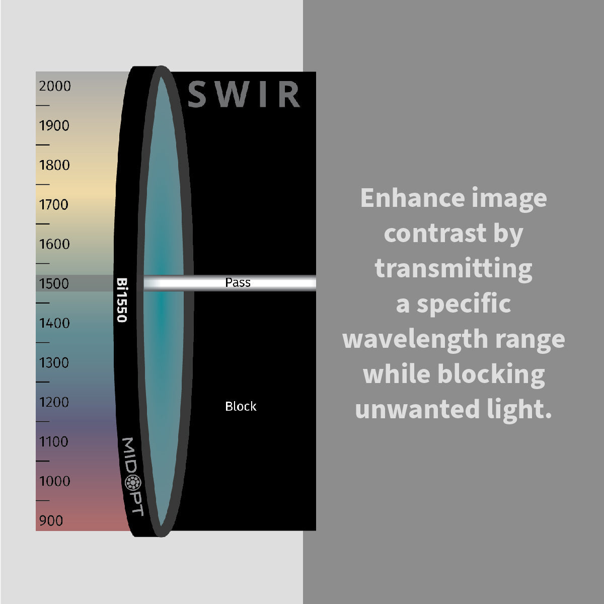
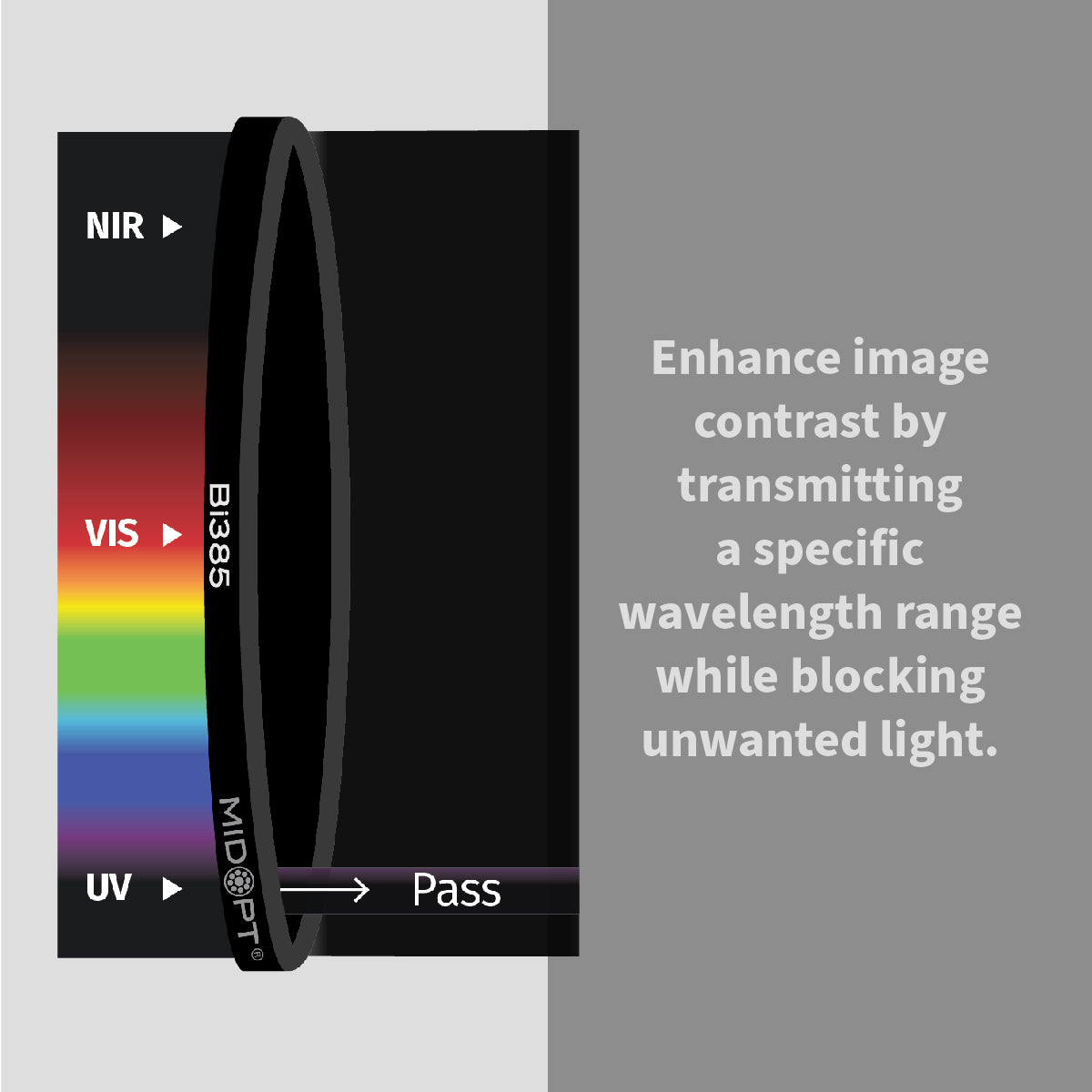
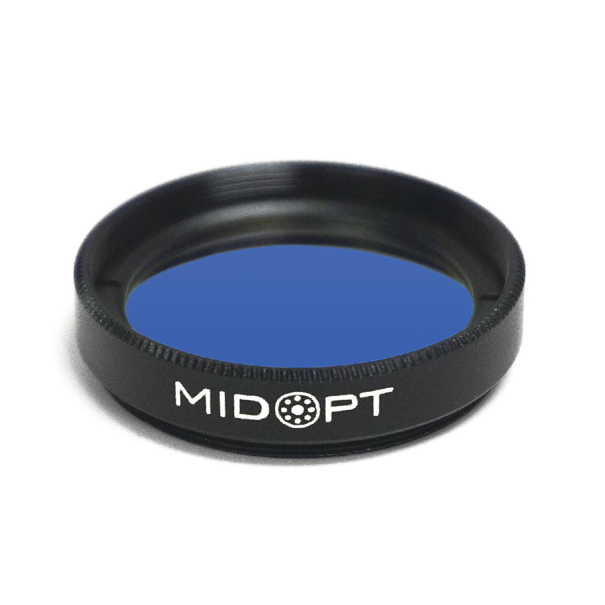
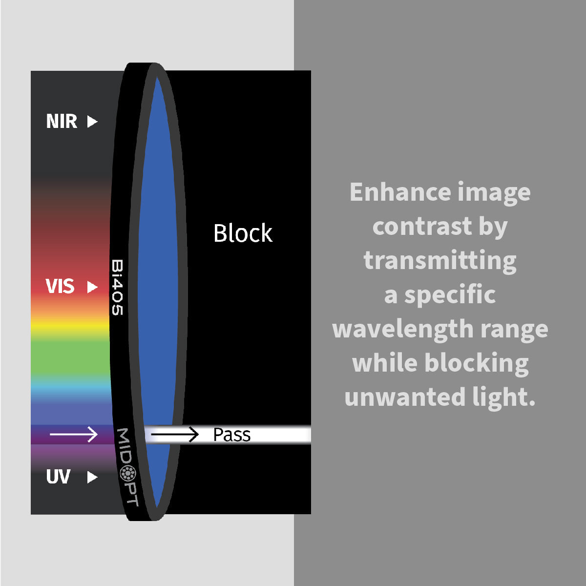
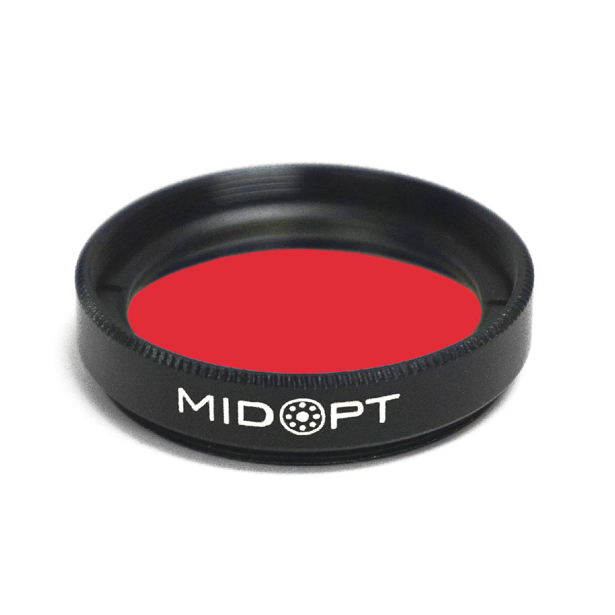
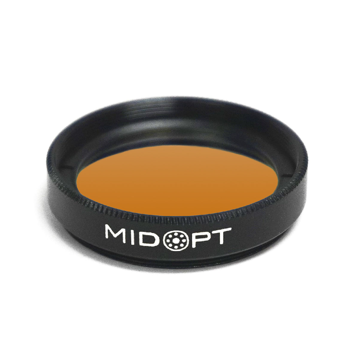
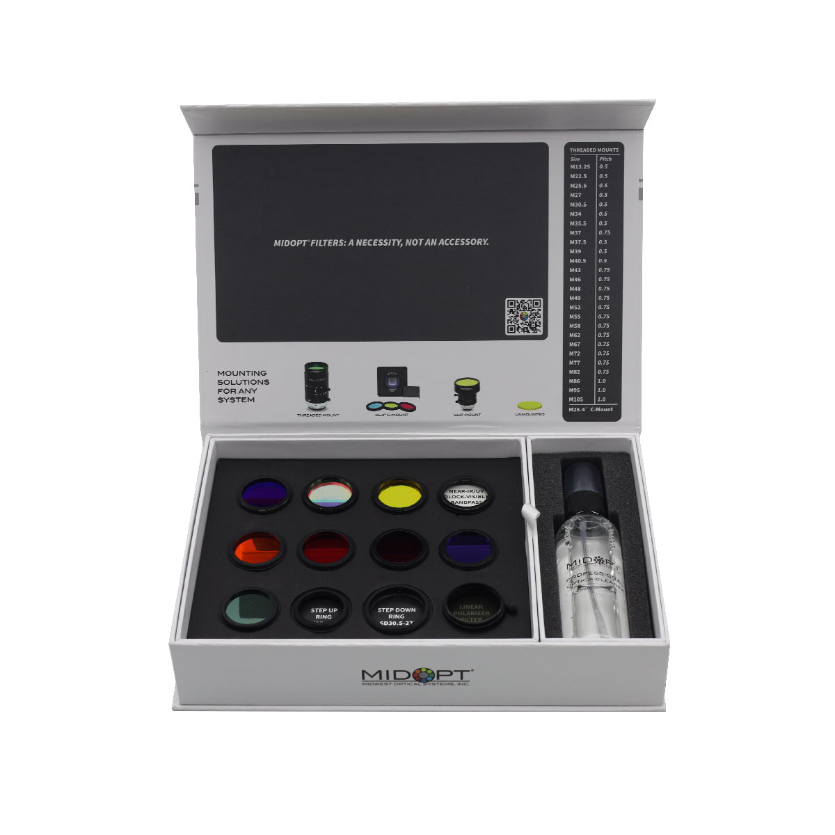
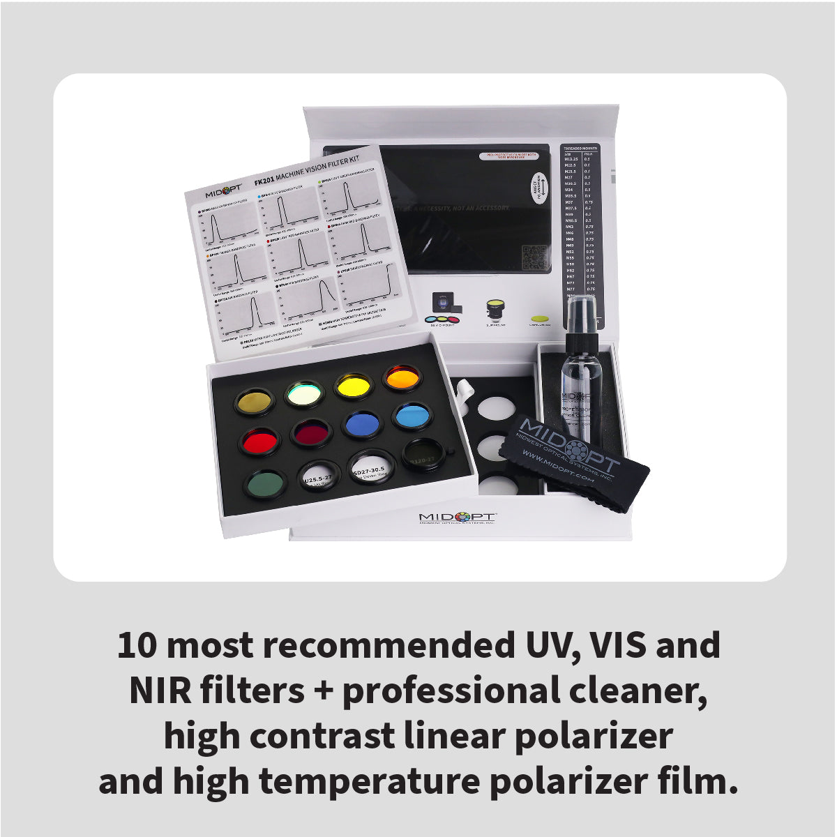
- Optical filters
- Image processing software
At FJW Optical, we offer a complete portfolio of machine vision components from industry-leading manufacturers, including JAI cameras, GOYO lenses, Theia lenses, MidOpt optical filters and CCS lighting solutions.