$15.00
$15.00


 Find-R-Scopes

 Filters
 Lenses
 Cameras
 Lighting


 Accessories










In the food processing industry, maintaining consistent product quality while meeting high production demands is essential. From sorting fresh produce to detecting contaminants and identifying defects, automated food inspection systems help manufacturers improve efficiency, reduce waste and maintain product standards.

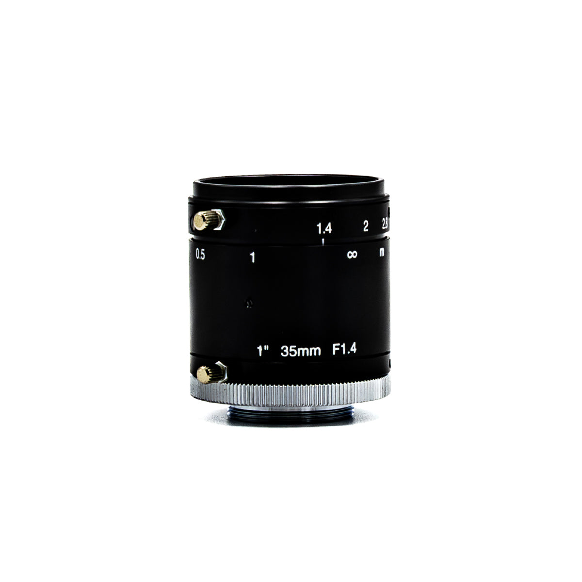
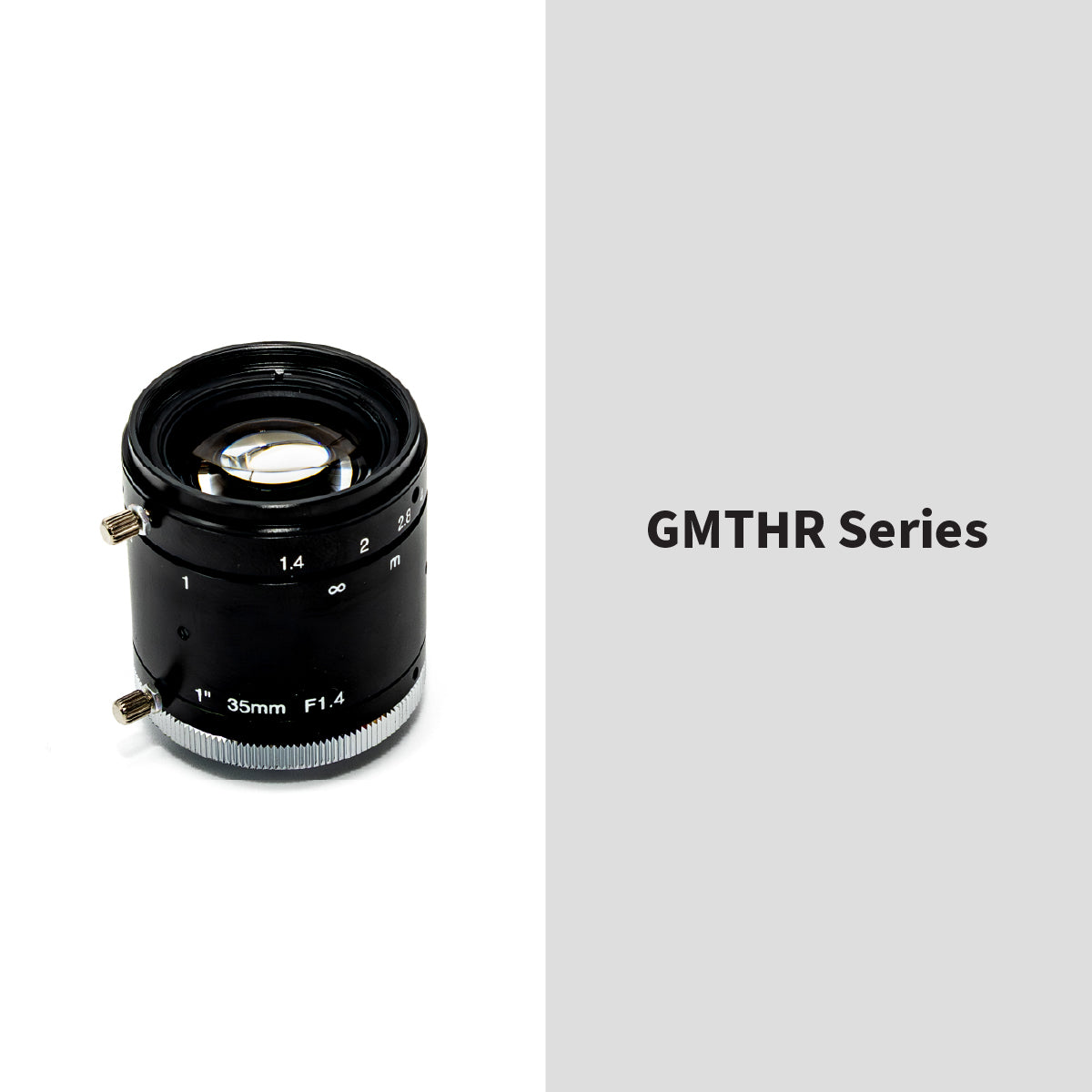
A robotic vision system is only as effective as the image it delivers. While camera resolution, lighting and image-processing software receive significant attention, the machine vision lens plays an equally important role in determining what the camera can see and how accurately the system can interpret it.

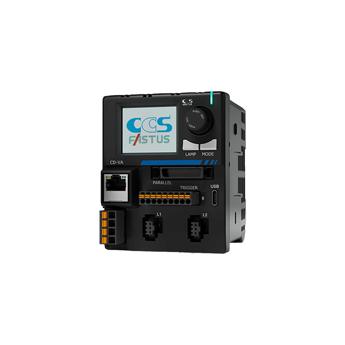
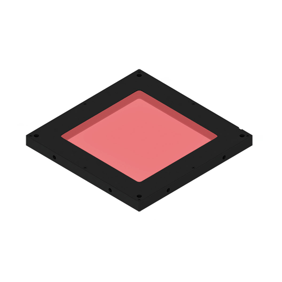
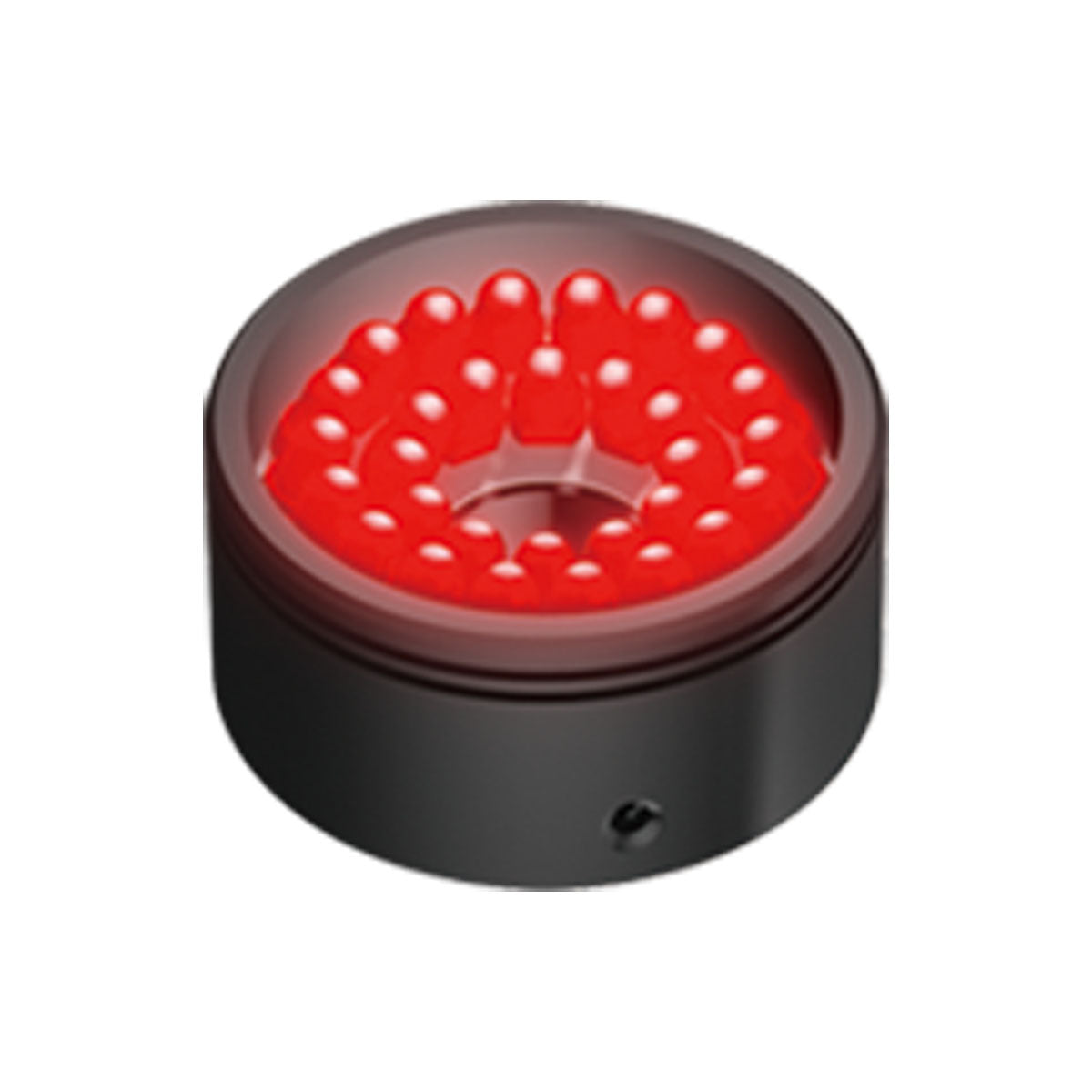
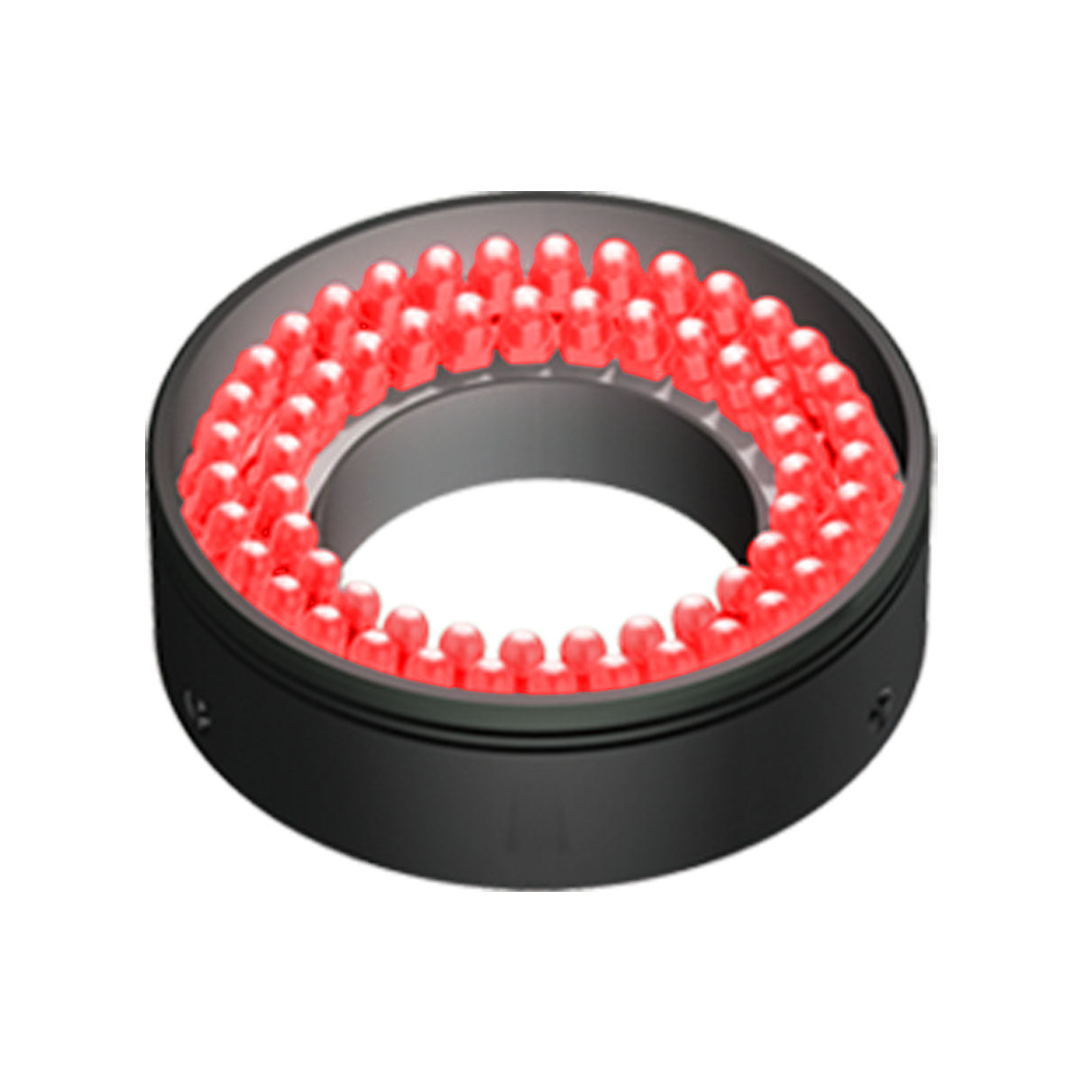
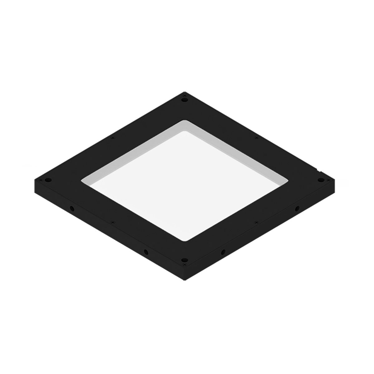
Robotic vision systems depend on more than cameras and software. The quality, direction and consistency of illumination can determine whether a vision system clearly identifies an object or struggles with shadows, reflections and insufficient contrast.

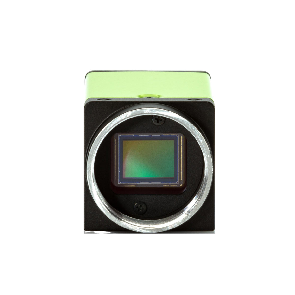
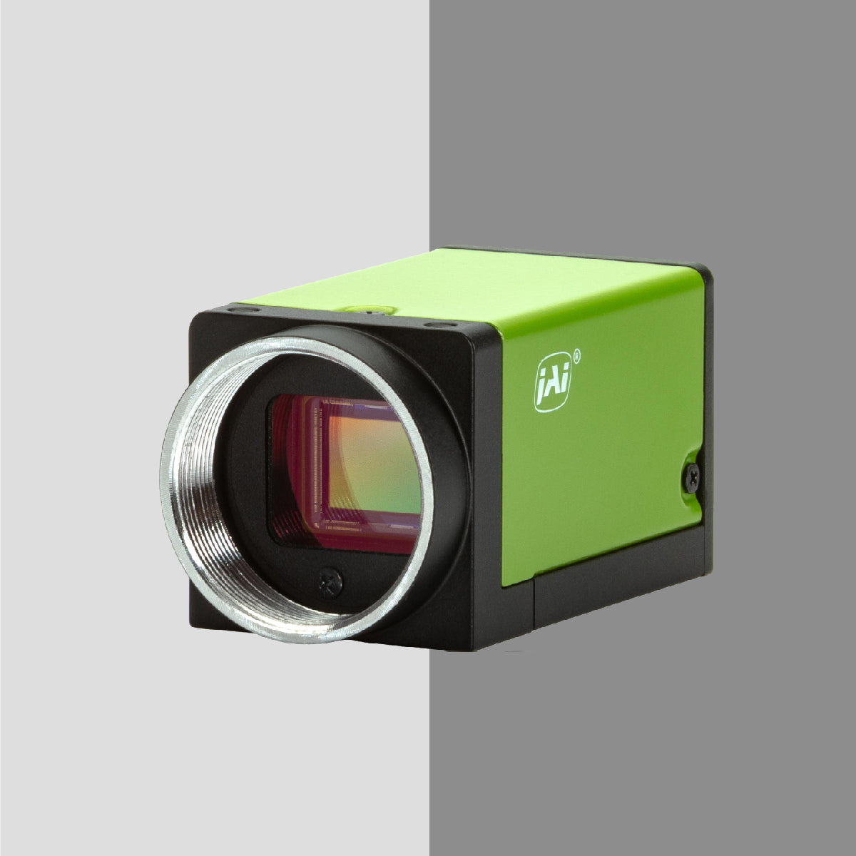
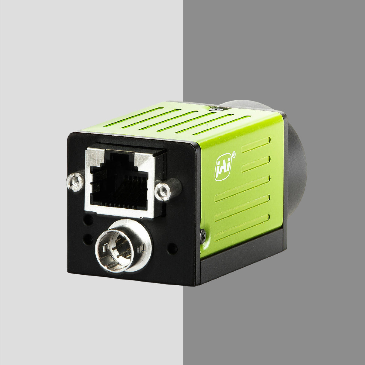
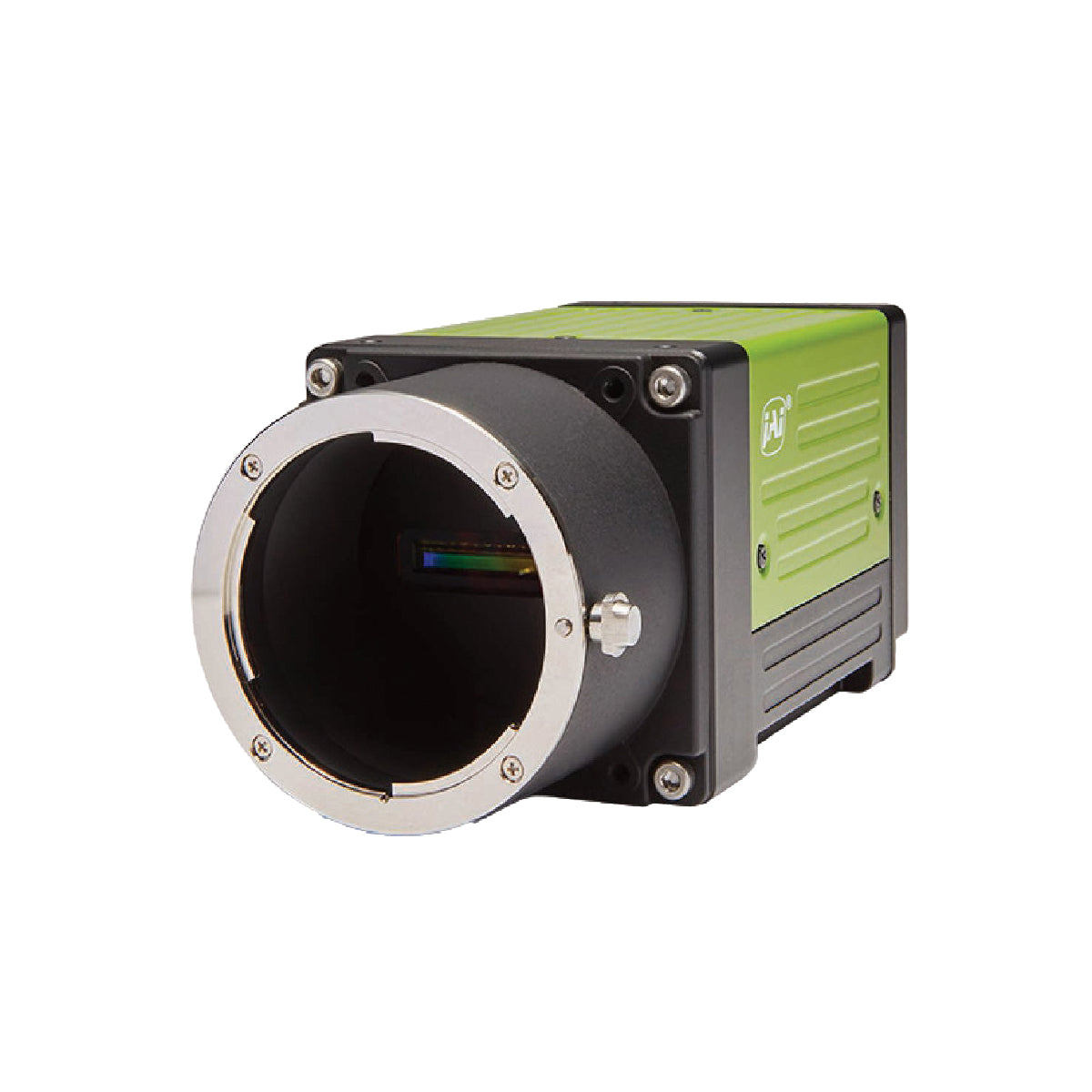
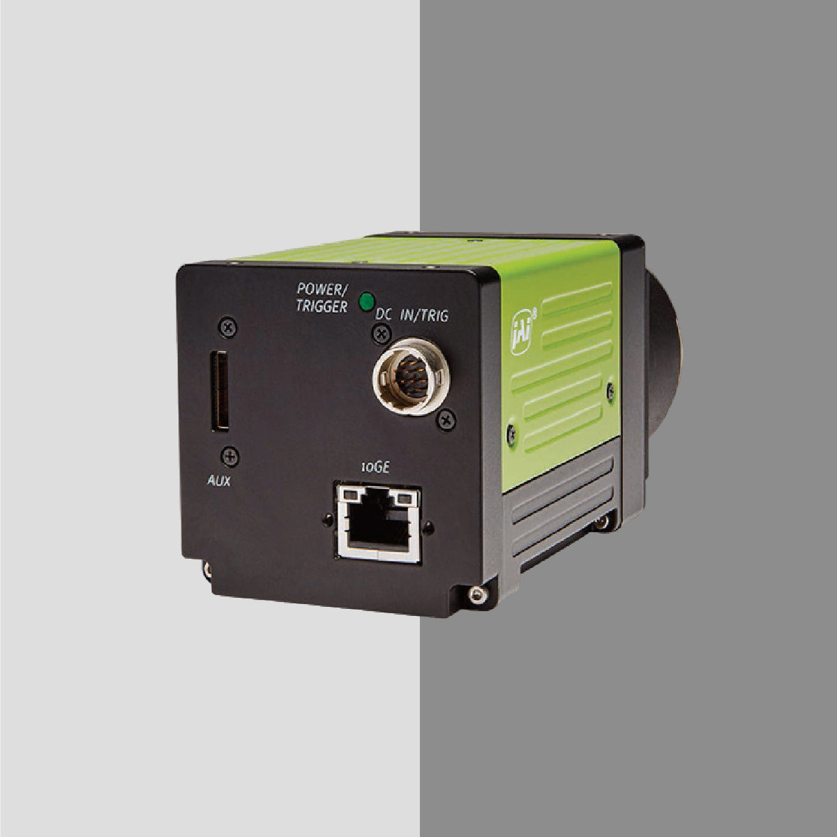
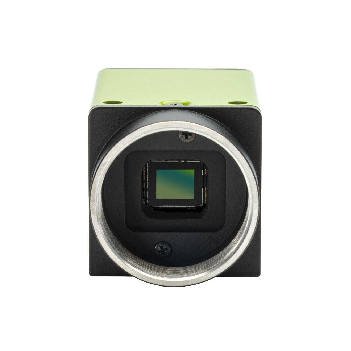
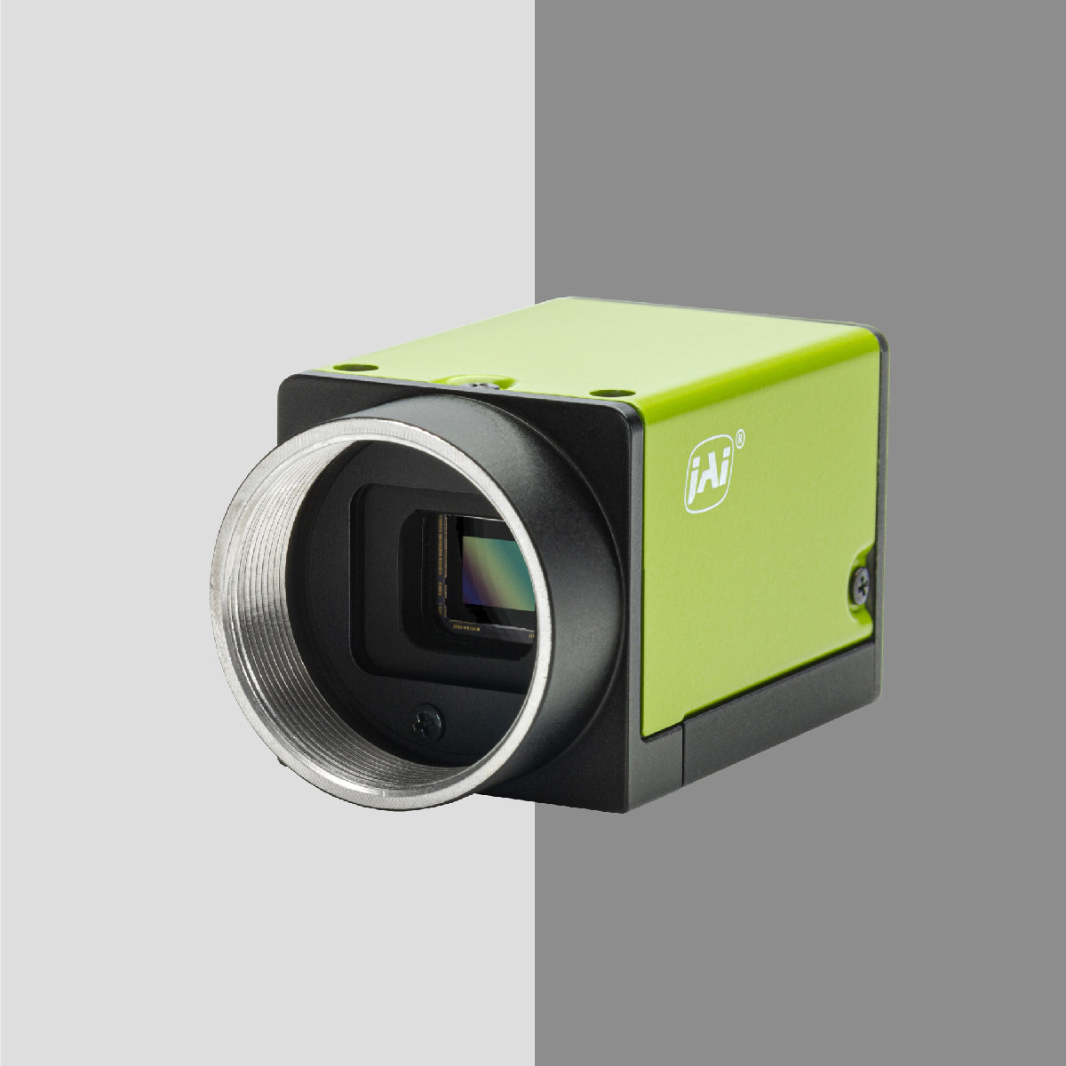
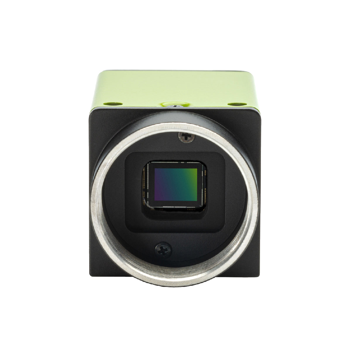
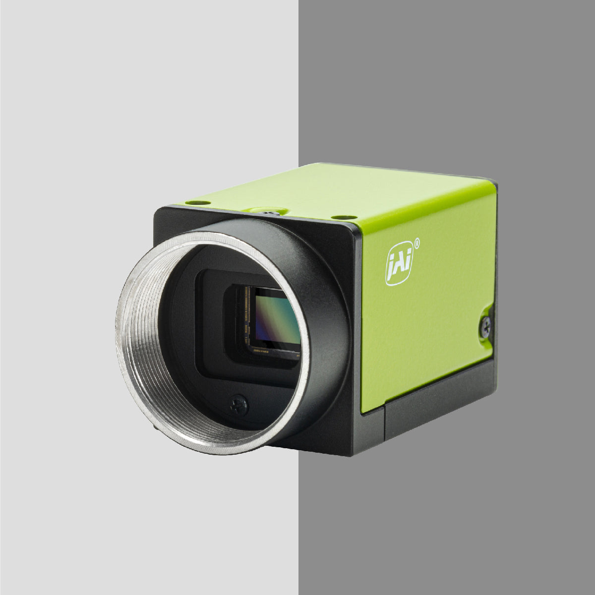
Modern robots are fast, precise and increasingly adaptable, but they still need reliable visual information to understand their surroundings. In robotic guidance and pick-and-place systems, industrial machine vision cameras serve as the eyes of the robot, providing the image data needed to locate parts, determine orientation, verify placement and make automated decisions.

Innovations in industrial imaging since 1969
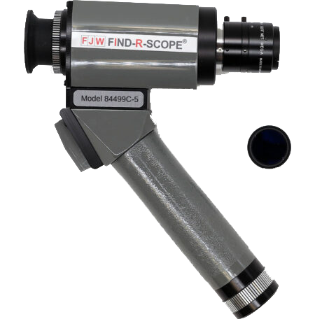
FJW Optical has a rich history of innovation in the optical industry. Early on, the company was a leader in manufacturing optical components for military applications and grew to pioneer the development of user-friendly infrared viewers, including the iconic Find-R-Scope. FJW expanded into telecommunications with the rise of fiber optics, and today remains on the forefront of technological advancements with the SWIR View, a handheld viewer designed for various applications in the short-wave infrared spectrum.

The most popular products from industry leaders
Shop a wide range of products from globally recognized brands in the machine vision industry.