
 Find-R-Scopes

 Filters
 Lenses
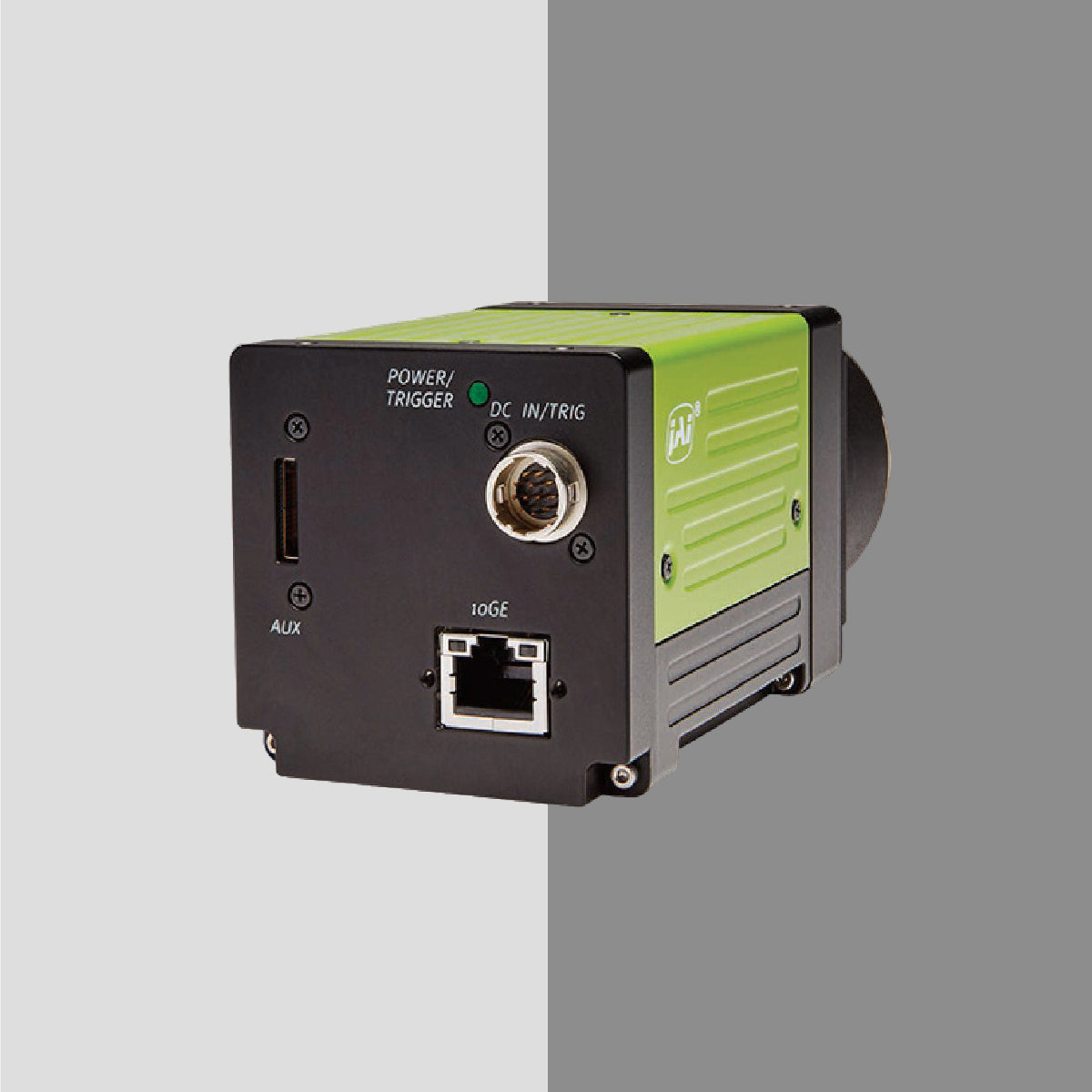
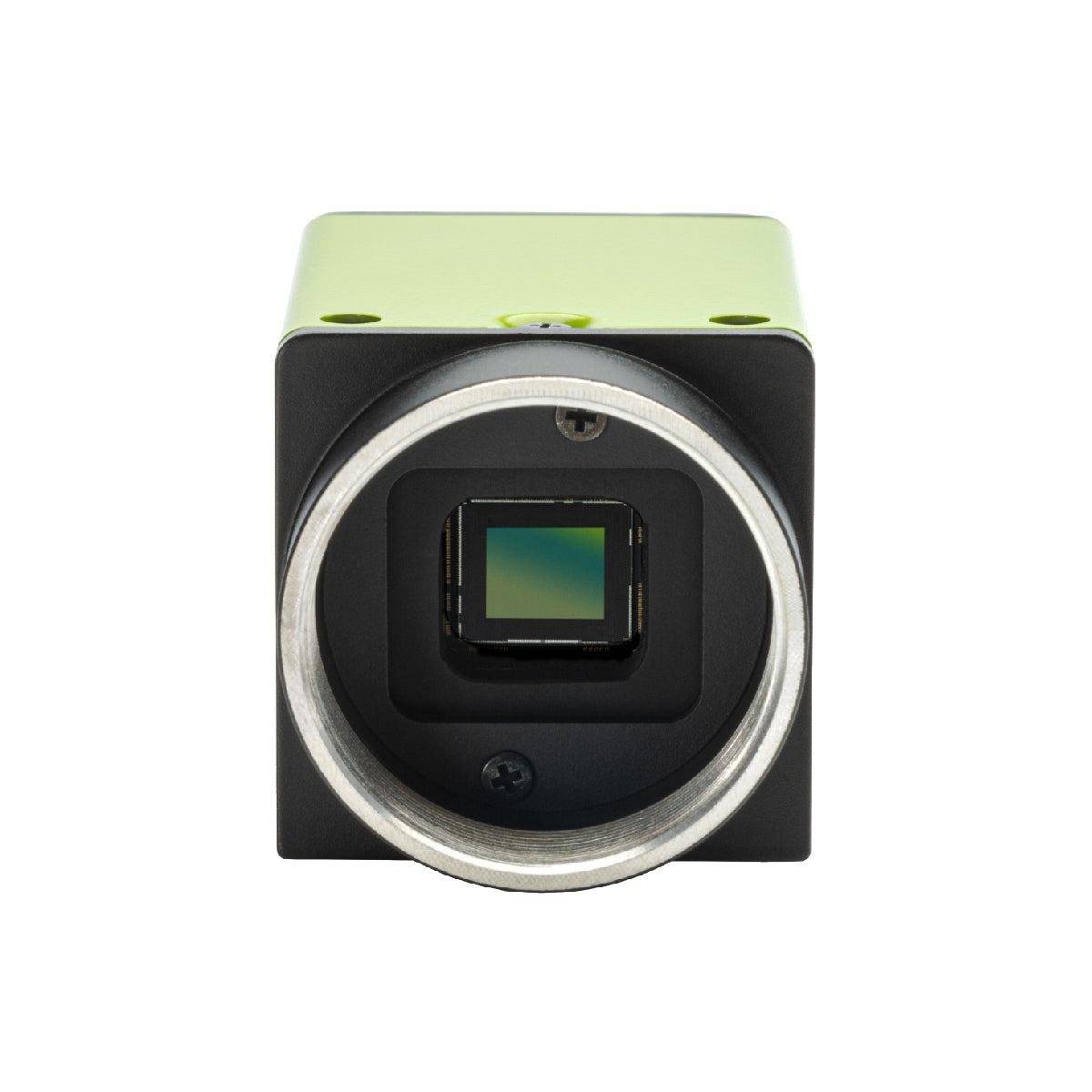
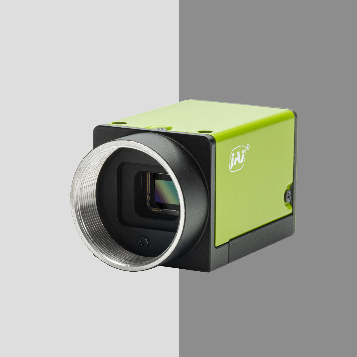
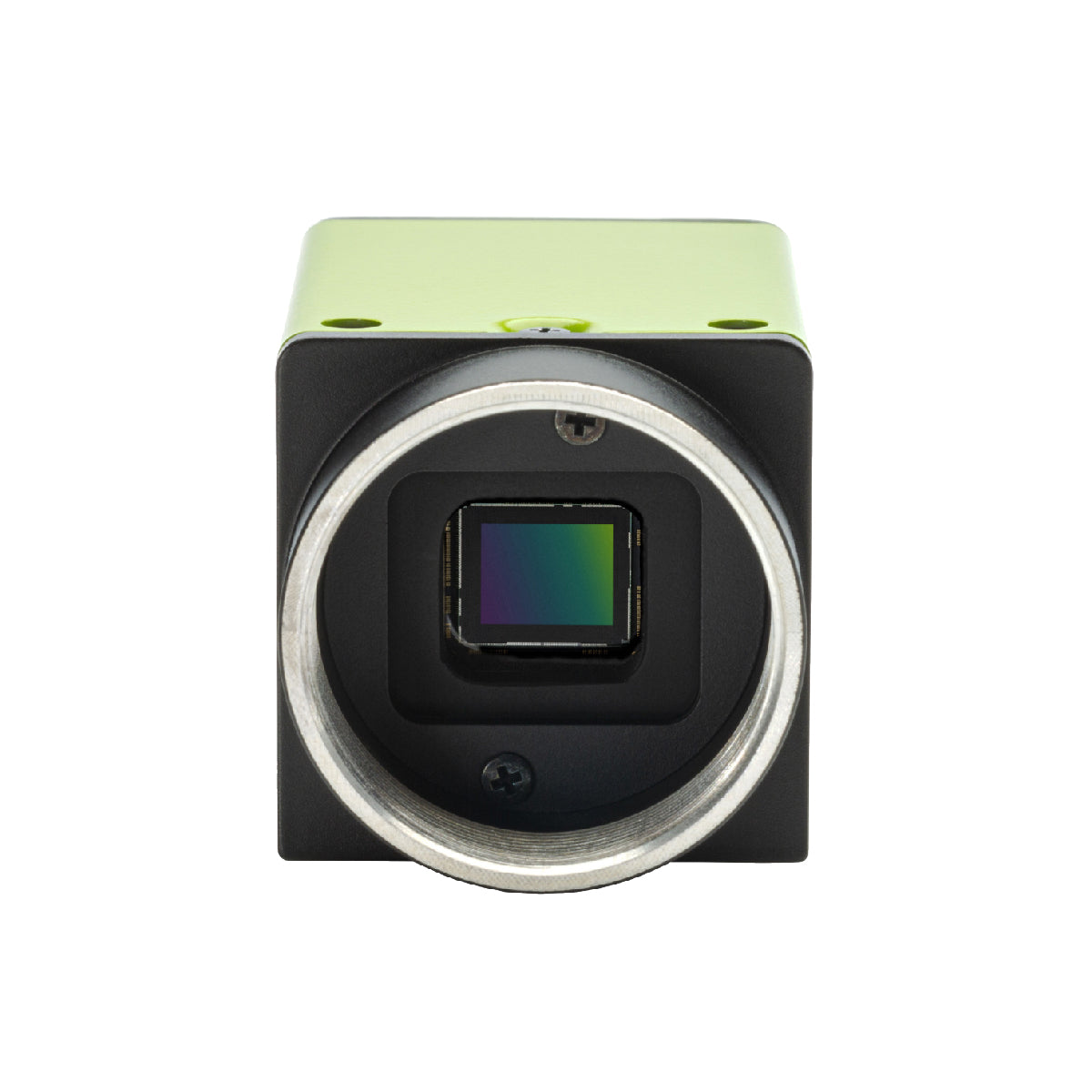
 Cameras
 Lighting

 Accessories









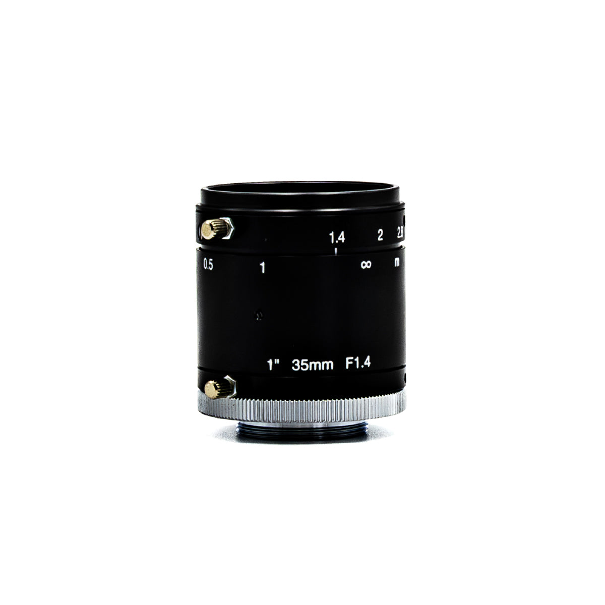
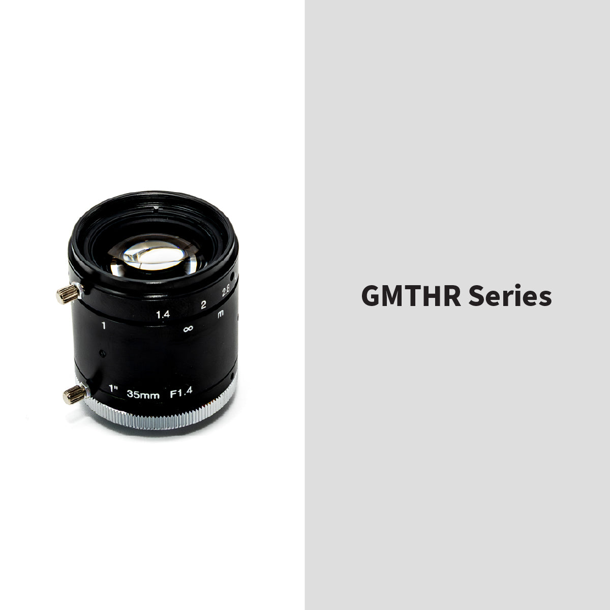


From printed circuit board (PCB) inspection and component placement verification to solder joint analysis and semiconductor inspection, the lens is a critical part of achieving reliable image quality.
Selecting a high-resolution camera is only part of the equation. If the lens cannot resolve the level of detail captured by the sensor, the system may produce images that appear soft, reduce edge definition and make small defects more difficult to identify.
Why Lens Resolution Matters in Electronics Inspection
Electronics inspection often requires detecting extremely small features, including fine PCB traces, component leads, solder bridges, cracks, scratches, contamination, alignment errors and printing defects.
A machine vision lens must transfer enough detail from the object to the camera sensor for the inspection software to distinguish these features consistently. The higher the inspection resolution required, the more important the optical performance of the lens becomes.
Using a high-megapixel camera with an inadequately resolved lens can effectively create a bottleneck. The sensor may have enough pixels to capture the defect, but the optical system may not deliver sufficient contrast and detail to those pixels.
For this reason, machine vision lens resolution should be considered together with camera resolution, sensor size, pixel size, field of view and the smallest feature that must be detected.
Megapixels Are Only Part of the Specification
Lens manufacturers commonly specify lenses by megapixel rating, but megapixels alone do not provide a complete picture of optical performance.
Resolution may also be expressed in line pairs per millimeter (lp/mm). This measurement describes the lens's ability to distinguish closely spaced details. As pixel sizes decrease and camera resolutions increase, the lens must typically provide greater resolving capability.
High-resolution fixed-focal machine vision lenses are available across a wide range of performance levels. For example, current industrial lens families include approximately:
- 5 MP lenses with resolution around 160 lp/mm
- 6 MP lenses with resolution around 170 lp/mm
- 10 MP lenses with resolution around 200 lp/mm
- 12 MP lenses reaching approximately 260 lp/mm
These specifications illustrate how optical resolution requirements increase as machine vision systems move toward higher-resolution sensors.
Match the Lens to the Camera Sensor
One of the most important rules when designing an electronics inspection vision system is to make sure the lens is capable of supporting the camera.
A 12MP camera does not automatically produce 12MP worth of usable inspection detail if the selected lens was designed for substantially lower-resolution imaging.
Sensor format is equally important. The lens image circle must cover the sensor while maintaining sufficient image quality from the center to the edges. High-resolution lenses are available for common machine vision formats including 2/3", 1", 1.1" and larger sensors. For example, 12MP fixed-focal lenses designed for 1" sensors can provide resolution ratings up to 260 lp/mm.
For PCB and electronics inspection, edge-to-edge performance can be particularly important because components located near the perimeter of the field of view still need to be inspected accurately.
Start With the Smallest Defect You Need to Detect
Rather than selecting a lens based only on camera megapixels, begin with the application.
Ask: What is the smallest feature or defect the machine vision system must reliably identify?
Depending on the electronics inspection process, this could include:
- Fine PCB traces and spacing
- Solder bridges or insufficient solder
- Bent or missing component leads
- Component positioning and orientation
- Surface scratches and cracks
- Connector pin alignment
- Printed characters, codes and markings
- Foreign material or contamination
Once the minimum feature size is established, engineers can determine the required object-space resolution and select the appropriate camera, lens, working distance and field of view.
A system inspecting an entire PCB for missing components, for example, may have very different optical requirements than a system examining individual solder joints or semiconductor features.
Pixel Size and Modern High-Resolution Sensors
Modern industrial cameras continue to offer higher pixel densities and smaller pixels. While this allows more detail to be captured within a given sensor area, it also places greater demands on the lens.
A lens designed for lower-resolution cameras may not provide sufficient contrast at the spatial frequencies required by a newer sensor. This is why simply upgrading the camera without evaluating the optics may provide less improvement than expected.
For demanding high-resolution electronics inspection, the camera and lens should be treated as one imaging system rather than separate components.
Field of View vs. Inspection Detail
Electronics manufacturers frequently want to inspect as much of a PCB or assembly as possible in a single image. Increasing the field of view can improve throughput, but it also spreads the camera's available pixels across a larger area.
For example, if the same camera is used to inspect progressively larger areas, fewer pixels are available to represent each millimeter of the object.
This creates an important design tradeoff:
Larger field of view = fewer pixels per feature
Smaller field of view = greater detail per feature
A higher-resolution camera and appropriately matched lens can help increase the field of view while maintaining the resolution required to detect small defects.
Focal Length and Working Distance
Lens resolution is not the only consideration. Focal length, working distance and sensor format determine the field of view and influence how the vision system can be physically integrated into an inspection station.
Machine vision lens families are available with multiple focal lengths, allowing system designers to select optics around their required field of view and available working distance. High-resolution lens series, for example, may offer focal lengths ranging from wide-angle options around 5-8mm through 50mm and beyond.
Minimum object distance (MOD) should also be reviewed, particularly when cameras need to be installed close to the PCB or electronic assembly.
Don't Overlook Distortion
Dimensional inspection, component alignment and precision positioning applications can also be affected by lens distortion.
When software is measuring distances, verifying component positions or determining whether an electronic part falls within a specified tolerance, distortion can introduce measurement error. A lens with controlled distortion and strong resolution across the image can help improve repeatability.
Contrast Is Just as Important as Resolution
The ability to technically resolve two features does not necessarily mean the inspection system can reliably distinguish them.
Machine vision algorithms depend heavily on contrast. Small solder defects, subtle surface imperfections and fine PCB traces must stand out sufficiently from surrounding areas.
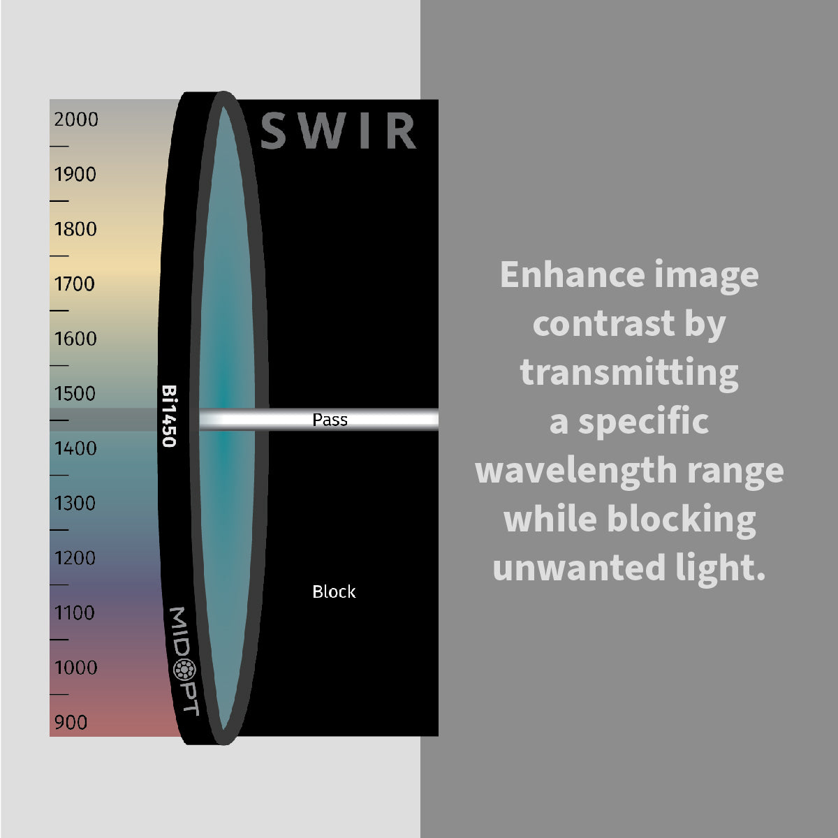
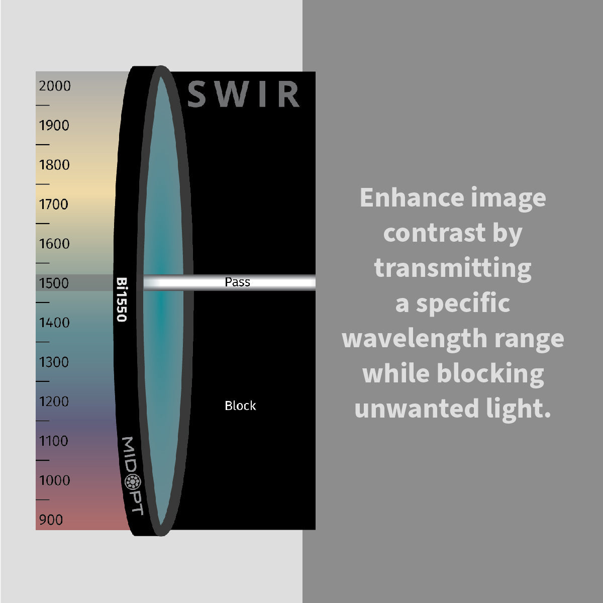
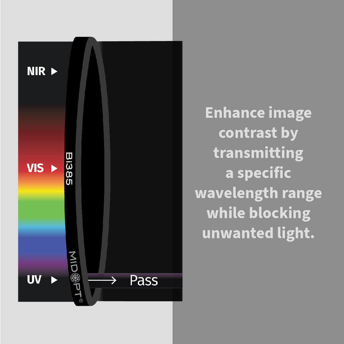
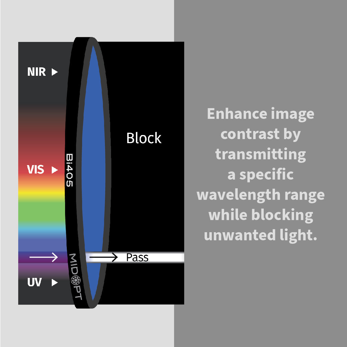
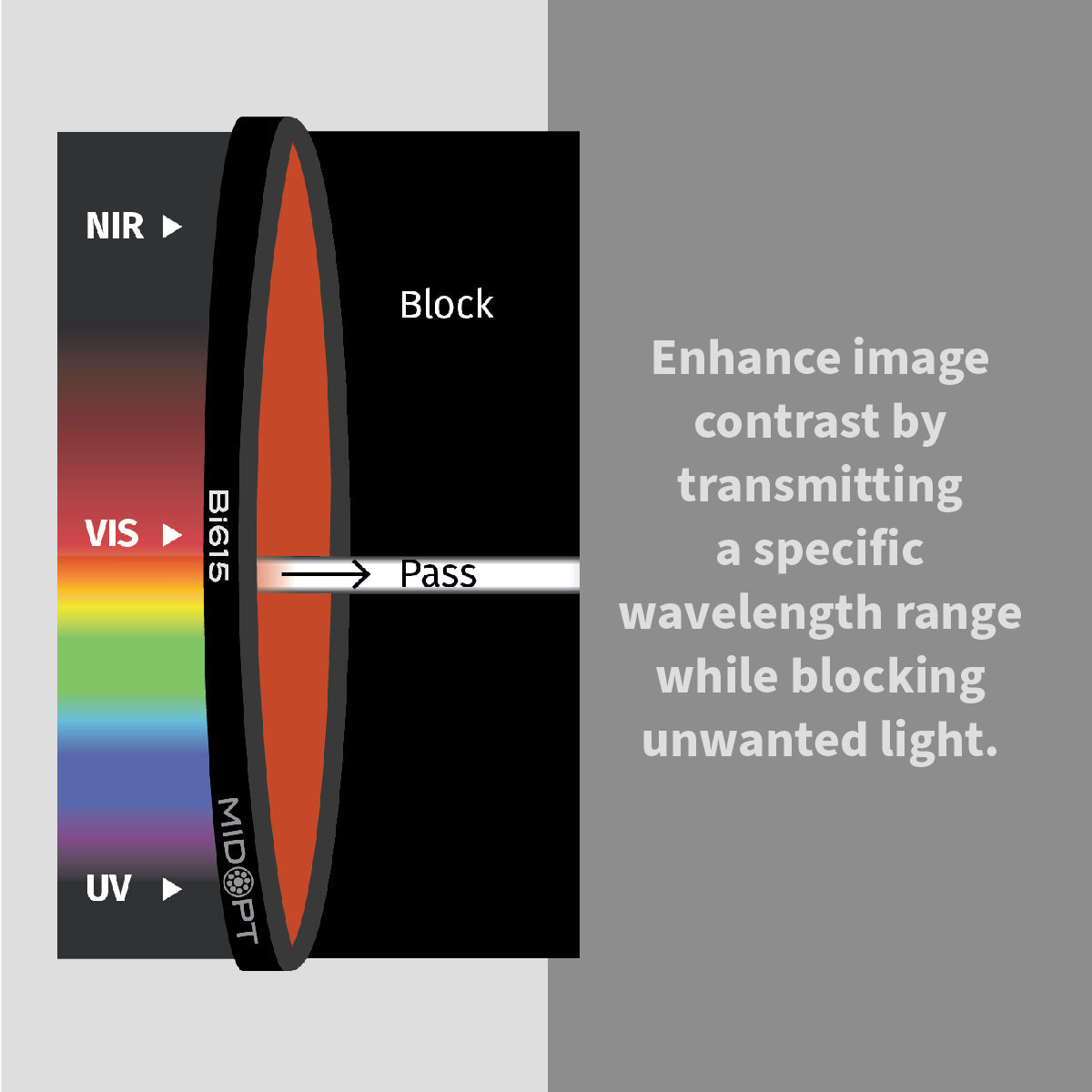
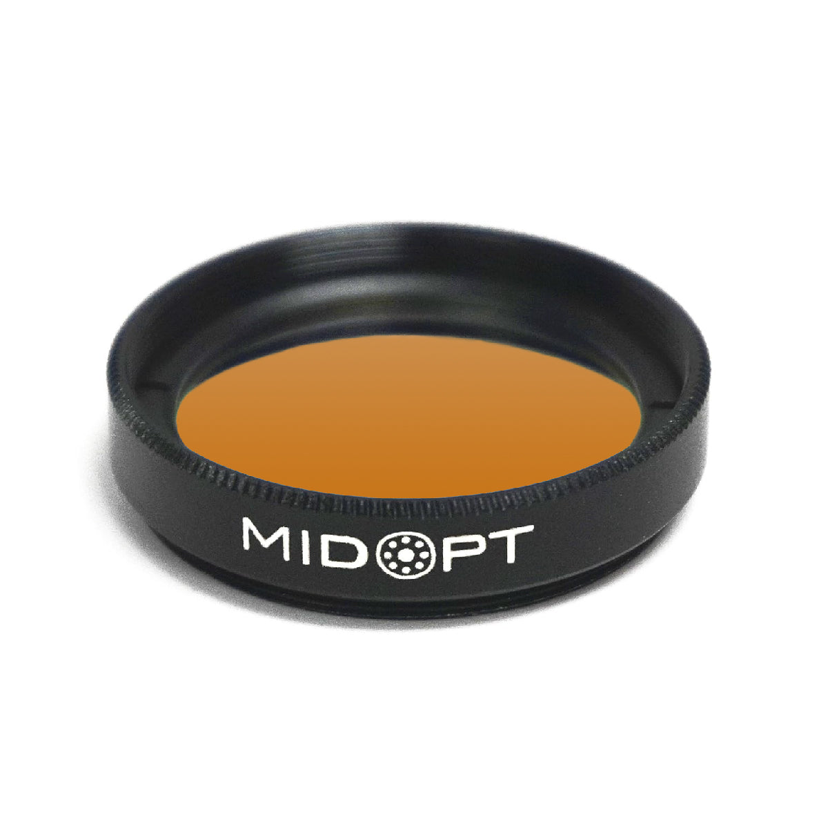
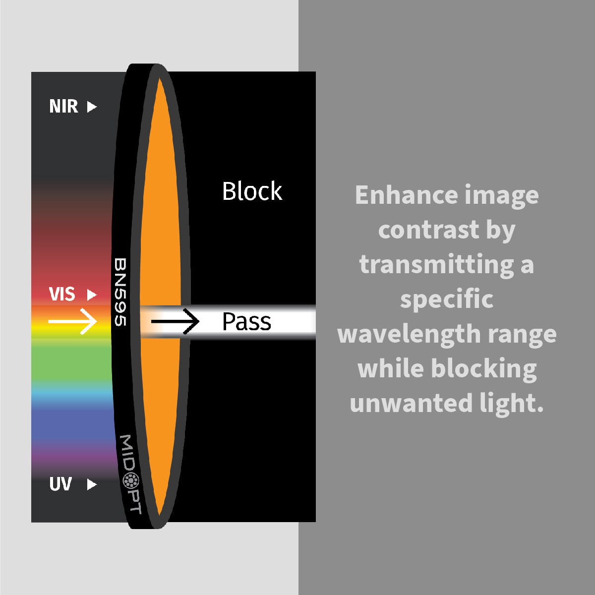
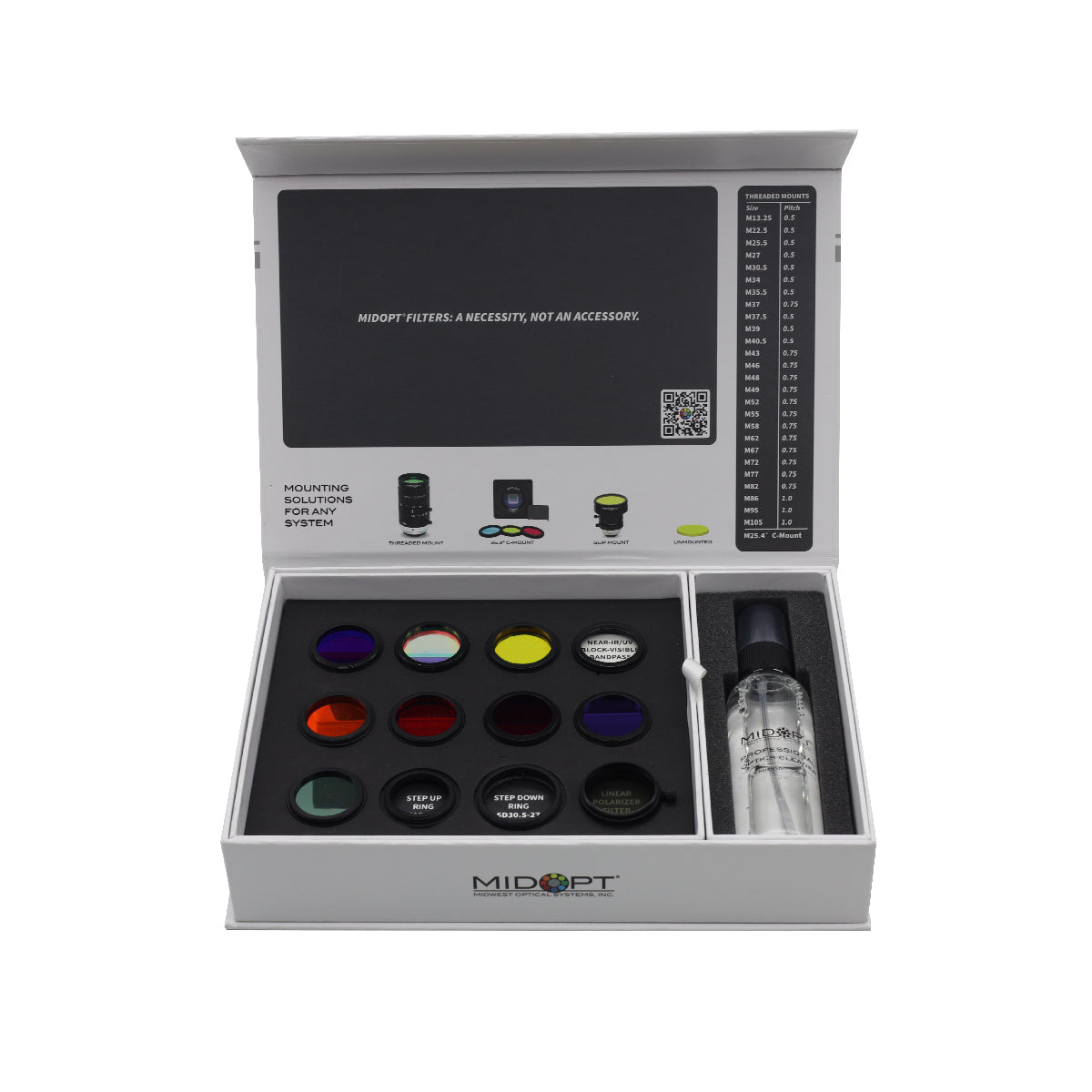
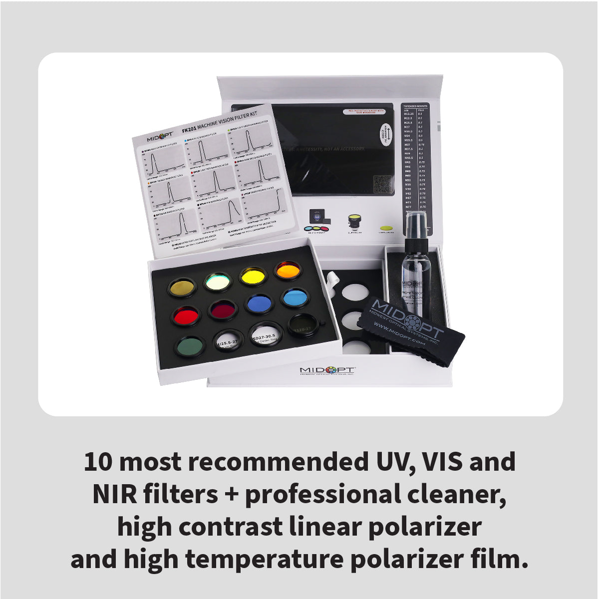
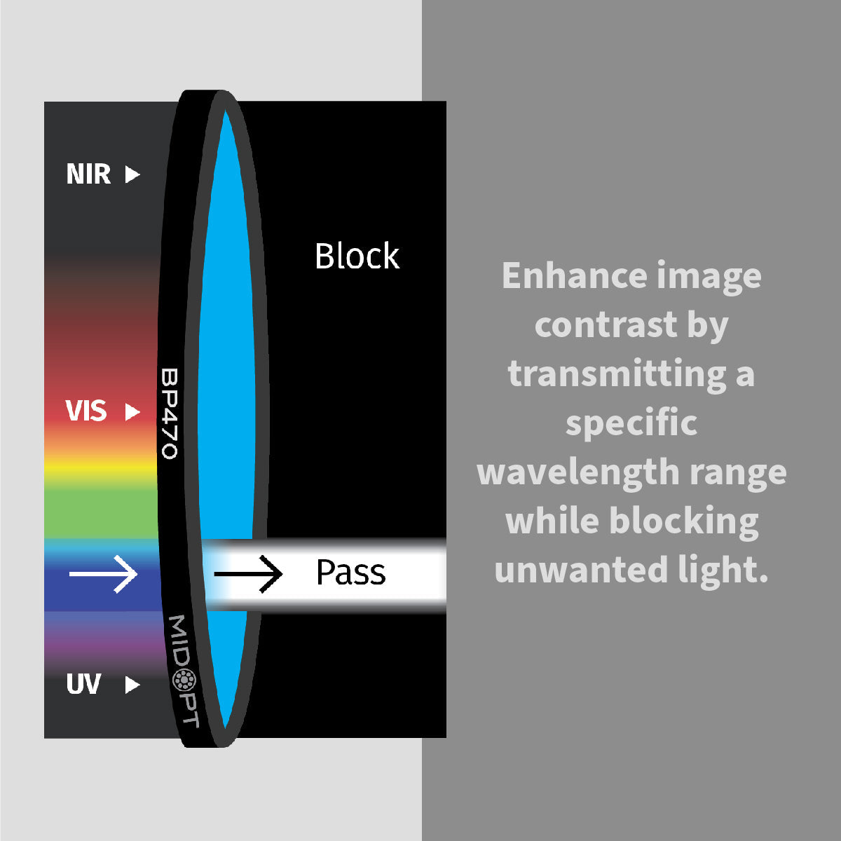
This is why lens resolution, lighting and optical filtration should be evaluated together. Proper illumination can emphasize the desired feature, while optical filters can improve contrast by controlling unwanted wavelengths, reflections or ambient light.
A high-resolution lens then preserves that contrast as the image reaches the sensor.
Choosing a Lens for PCB and Electronics Inspection
When specifying a machine vision lens for electronics inspection, consider the complete imaging system:
Camera resolution and pixel size: Make sure the lens provides sufficient optical resolution for the sensor.
Sensor format: Select a lens designed to cover the camera's sensor size.
Smallest detectable feature: Calculate whether enough pixels represent the smallest defect or feature of interest.
Field of view: Determine how much of the PCB, semiconductor or assembly must be captured in each image.
Working distance: Verify that the selected focal length provides the required field of view within the available installation space.
Optical resolution: Review both megapixel ratings and lp/mm specifications when comparing lenses.
Distortion: Consider distortion requirements for dimensional measurement and precision positioning.
Lighting and filtration: Optimize contrast before assuming that additional camera resolution alone will solve an imaging problem.
Building a Better Electronics Inspection System
High-resolution cameras have created new opportunities for faster and more detailed electronics inspection, but camera resolution alone does not determine system performance. The lens must be capable of delivering the detail that the sensor was designed to capture.
For PCB inspection, solder joint inspection, semiconductor manufacturing, component verification and other automated electronics applications, matching lens resolution, sensor resolution, field of view and working distance can improve defect detection and help create a more reliable machine vision system.
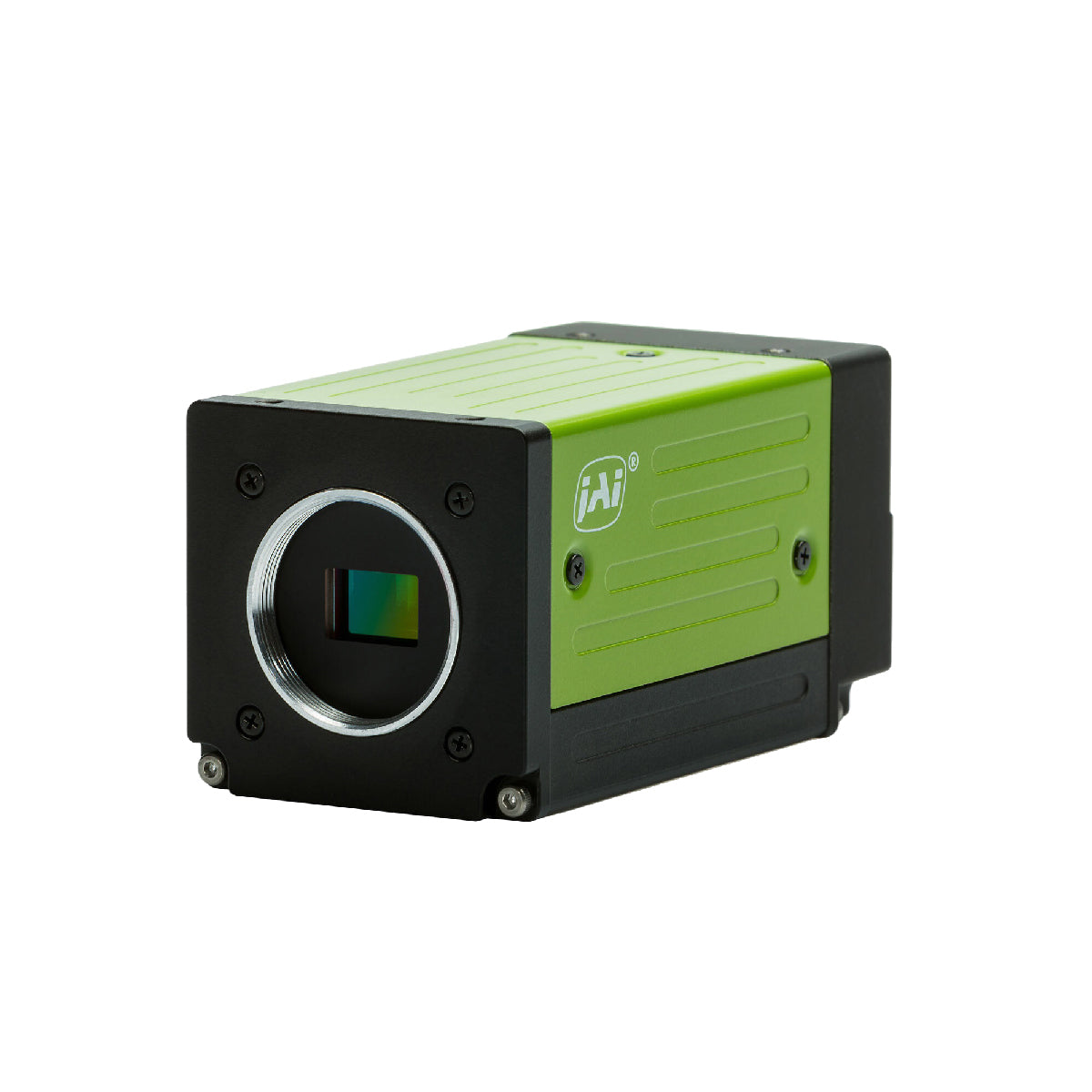
FJW Optical Systems offers a wide selection of machine vision lenses, industrial cameras, optical filters and LED lighting for electronics inspection and factory automation. Whether you are designing a new PCB inspection system or upgrading an existing vision platform, selecting compatible imaging components from the beginning can help maximize image quality and inspection performance.