
 Find-R-Scopes

 Filters
 Lenses
 Cameras
 Lighting


 Accessories












Printed circuit board (PCB) inspection is one of the most demanding applications in machine vision. As electronic assemblies become more compact and densely populated, manufacturers rely on automated optical inspection (AOI) systems to identify increasingly smaller defects while maintaining high production speeds.
One of the greatest challenges during PCB inspection is glare. Reflections from solder joints, copper traces, metallic components, and protective coatings can obscure critical features, reduce image contrast, and lead to missed defects or false rejects.
The right machine vision lighting is often the difference between a clear, repeatable inspection and inconsistent imaging. By selecting lighting that minimizes reflections and enhances feature visibility, manufacturers can significantly improve inspection accuracy and production efficiency.
Why Glare Is a Challenge in PCB Inspection
Electronic assemblies contain a wide variety of materials, each reflecting light differently. Common reflective surfaces include:
- Solder joints
- Copper pads and traces
- Gold-plated contacts
- Tin finishes
- Aluminum heat sinks
- Metal component leads
- Shielding cans
- Conformal coatings
When bright light reflects directly into the camera, important details may disappear beneath saturated highlights. Machine vision software can struggle to distinguish actual defects from reflections, resulting in unreliable inspections. Effective lighting controls these reflections before the image is ever captured.
The Importance of Lighting Geometry
The direction, angle, and shape of illumination play a major role in reducing glare. Instead of simply increasing light intensity, successful PCB inspection systems position illumination so that reflected light is directed away from the camera while useful image information remains visible. Carefully selected lighting geometry helps produce:
- Higher image contrast
- Better edge definition
- Reduced hotspots
- Improved defect visibility
- More consistent inspections
Optimizing lighting often provides greater performance improvements than increasing camera resolution alone.
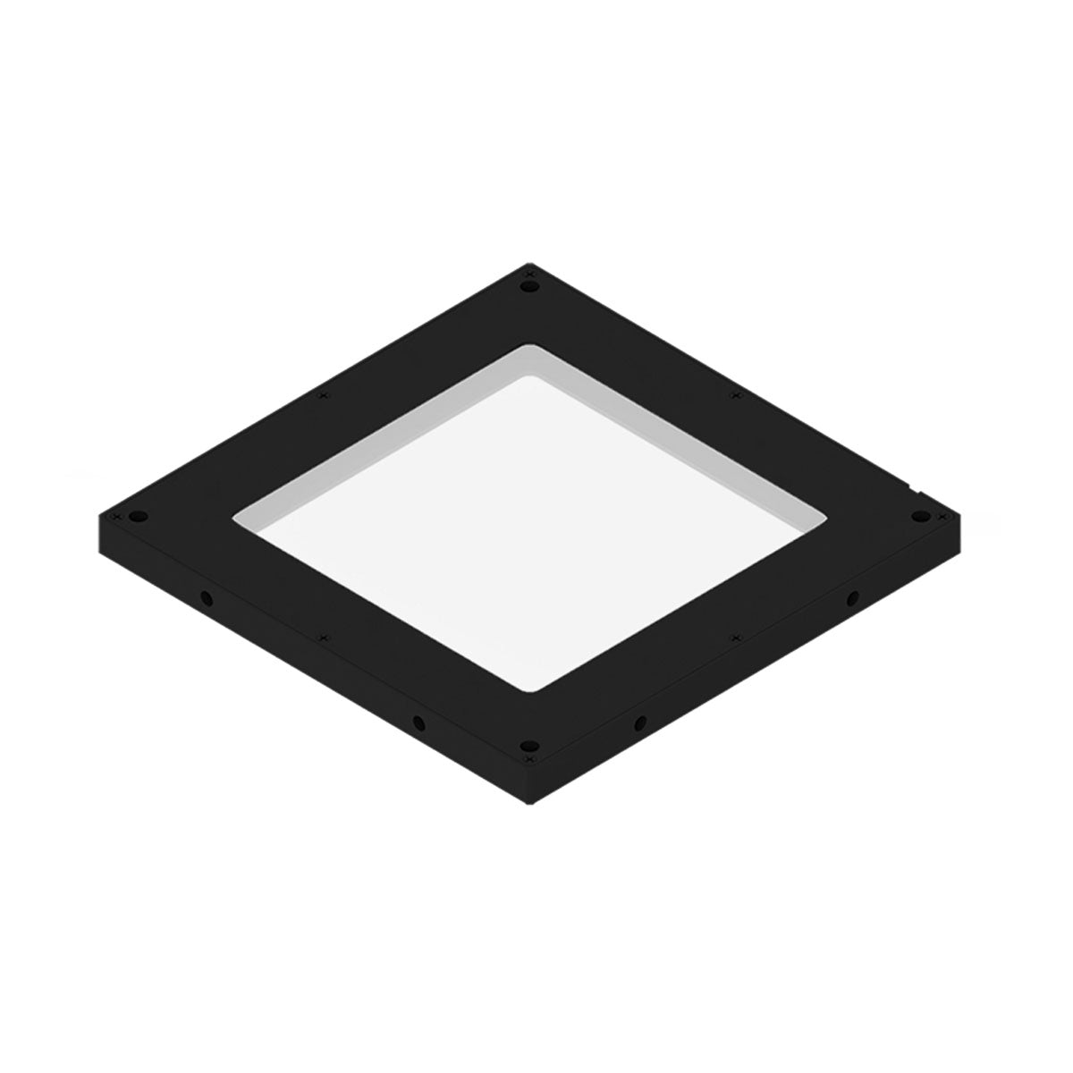
Diffuse Lighting for Uniform Illumination
Diffuse lighting spreads illumination evenly across the inspection area, reducing harsh reflections from shiny surfaces. This lighting method is particularly useful for inspecting:
- Populated PCBs
- Solder joints
- Surface-mount components
- Reflective metal finishes
- Mixed-material assemblies
Benefits include:
- Reduced specular reflections
- More uniform brightness
- Better visibility of fine details
- Improved image consistency
- Lower sensitivity to part orientation
Diffuse illumination is often one of the first solutions considered when inspecting reflective electronic assemblies.
Dome Lighting for Highly Reflective Surfaces
Highly reflective components can be especially difficult to inspect with conventional directional lighting. Dome lighting surrounds the target with evenly distributed illumination from multiple angles, producing soft, indirect light that minimizes glare.
Typical applications include:
- Solder joint inspection
- Connector inspection
- Metal shielding
- BGA package inspection
- Reflective electronic housings
Advantages include:
- Significant glare reduction
- Uniform lighting across complex assemblies
- Improved inspection repeatability
- Enhanced visibility of subtle surface defects
Dark Field Lighting for Surface Defects
While diffuse lighting reduces glare, dark field illumination highlights small surface irregularities. By directing light at a very low angle, only raised or damaged features reflect light into the camera.
Dark field lighting excels at detecting:
- Scratches
- Burrs
- Cracks
- Surface contamination
- Raised solder
- Foreign particles
- Damaged traces
This technique produces high contrast between defects and surrounding surfaces, making it ideal for identifying imperfections that may be difficult to detect under standard illumination.
Coaxial Lighting for Flat Reflective Surfaces
Many PCB inspection tasks involve flat reflective areas that require extremely uniform illumination. Coaxial lighting projects light directly along the camera's optical axis using a beam splitter, creating even illumination while minimizing shadows.
Applications include:
- Copper trace inspection
- Wafer inspection
- Flat electronic substrates
- Laser markings
- Printed text
- Surface inspection
This approach delivers exceptional image uniformity for flat reflective targets.
Low-Angle Ring Lighting
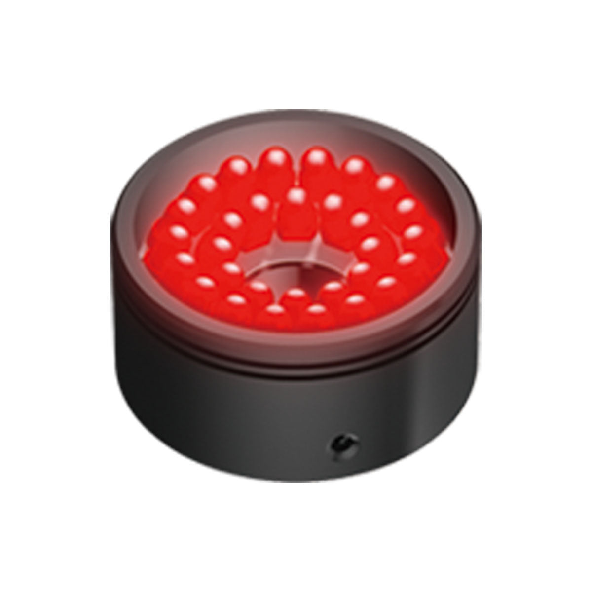
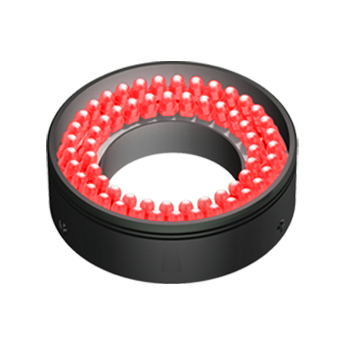
Ring lights remain one of the most versatile lighting solutions for electronics manufacturing. When configured at lower illumination angles, ring lights can reduce direct reflections while emphasizing component edges.
Common inspection tasks include:
- Component placement verification
- Lead inspection
- Connector alignment
- PCB assembly inspection
- OCR verification
- Barcode and Data Matrix reading
Different illumination angles can dramatically change how defects appear, making proper ring light selection essential.
Structured Lighting for Height Measurement
Some PCB inspection applications require three-dimensional information in addition to standard imaging. Structured lighting projects precisely controlled light patterns onto a surface, allowing machine vision systems to measure height differences.
Applications include:
- Solder paste inspection (SPI)
- Coplanarity measurement
- Lead height inspection
- Component height verification
- Connector positioning
- Package inspection
These techniques provide valuable dimensional information that cannot be obtained from conventional 2D imaging alone.
Combining Lighting with Optical Filters
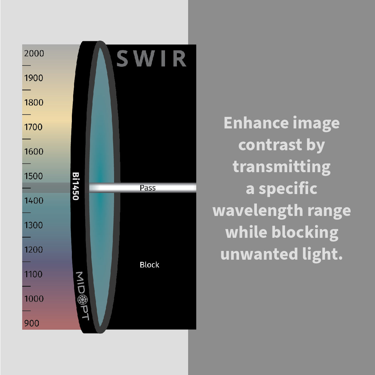
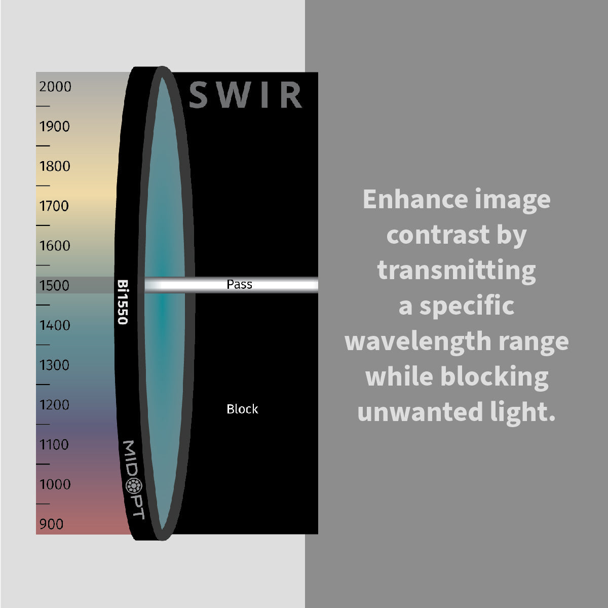
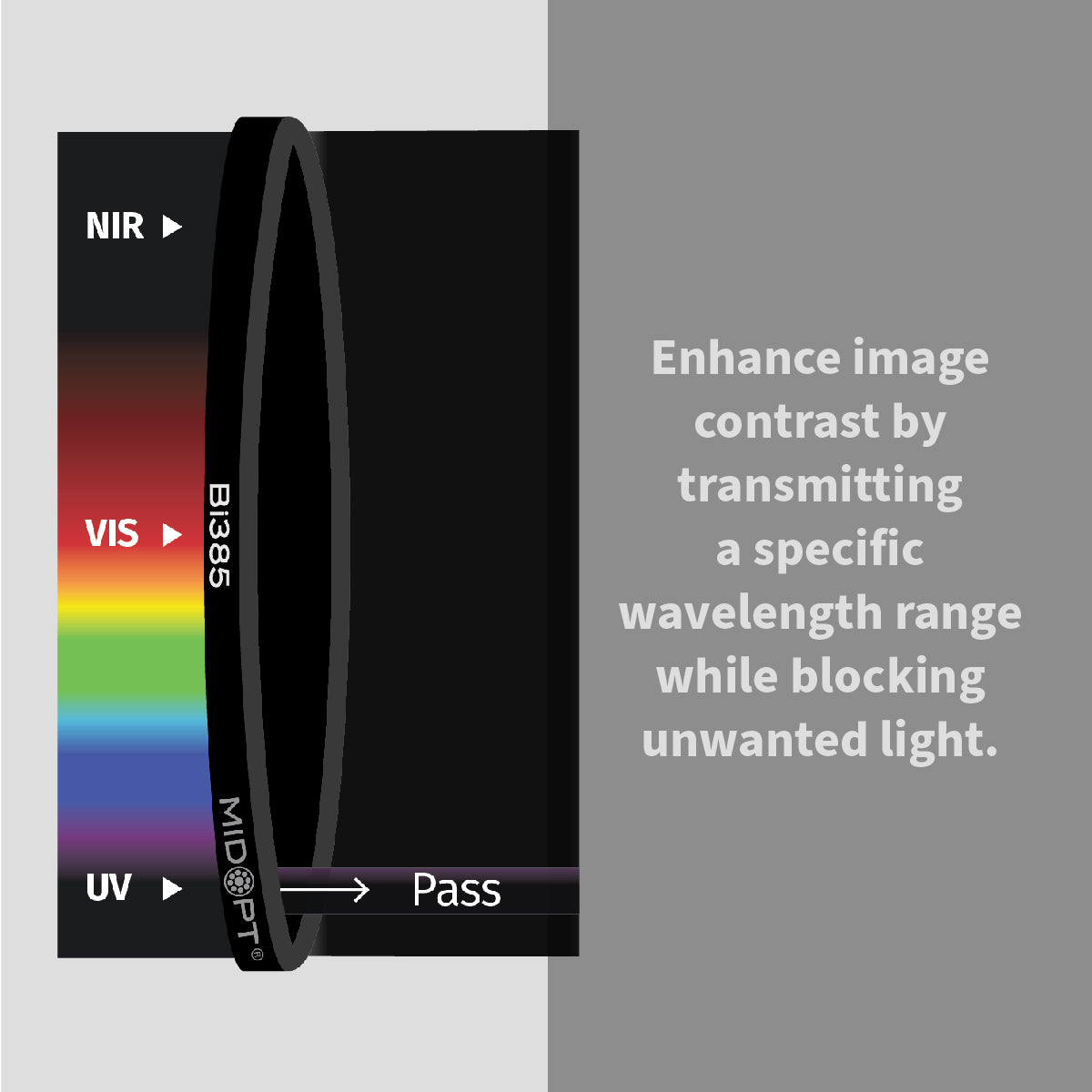
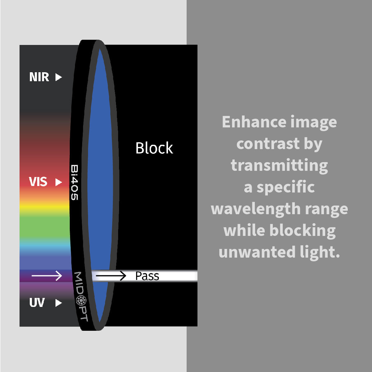
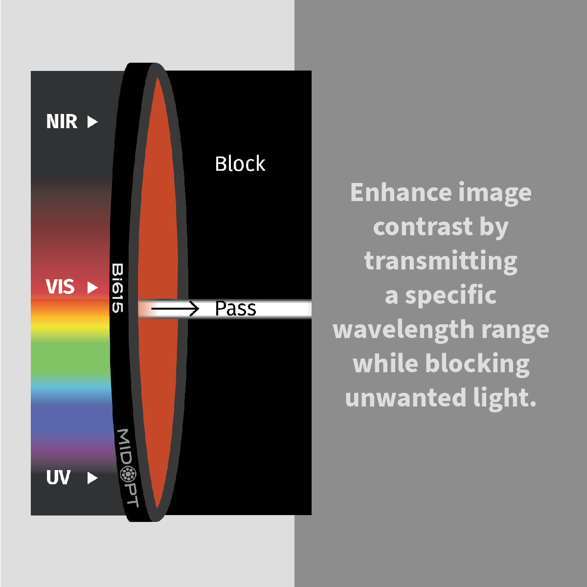
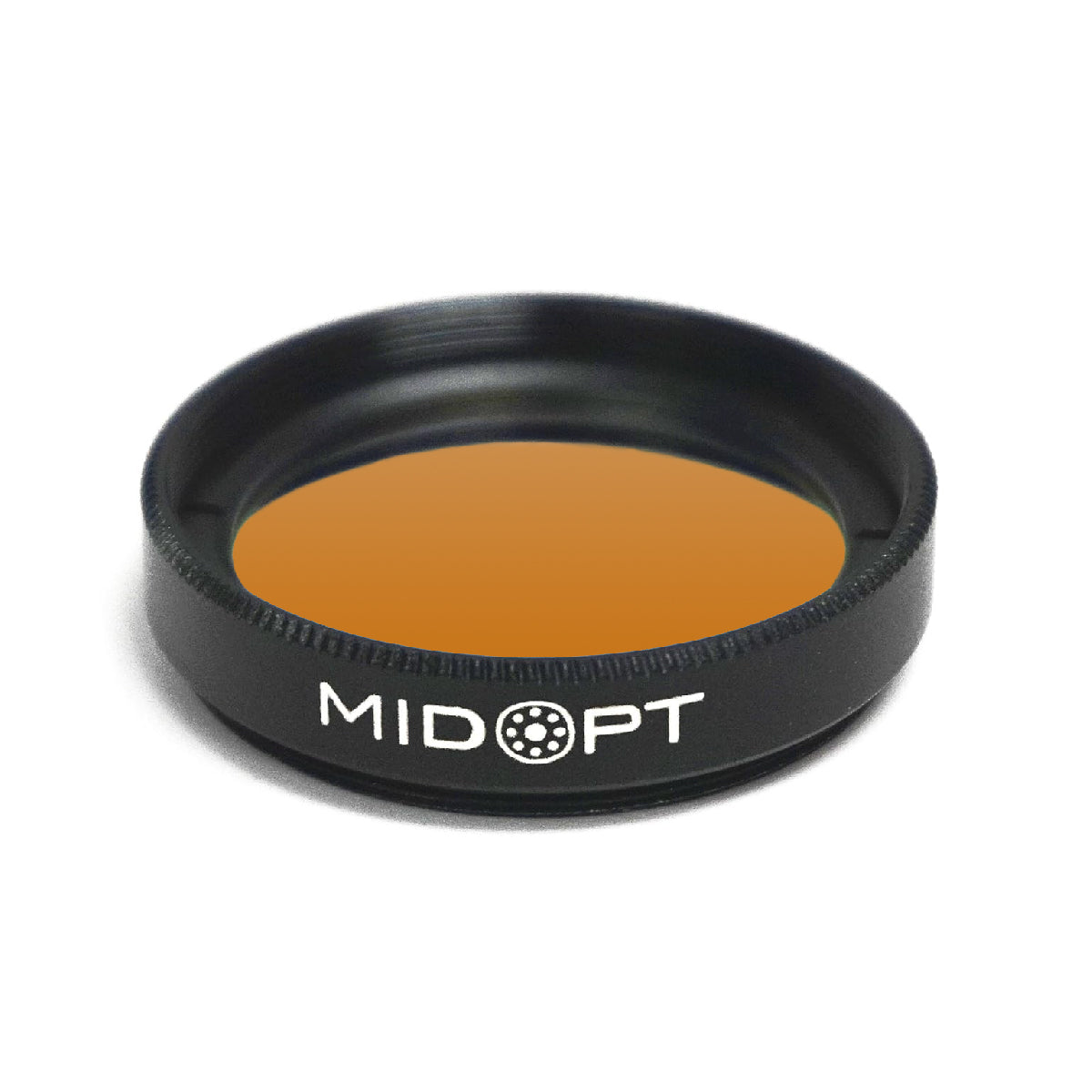
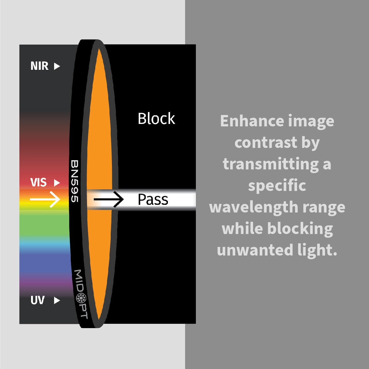
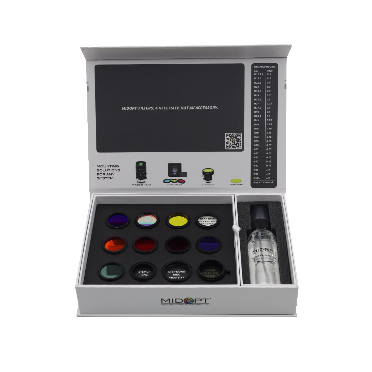
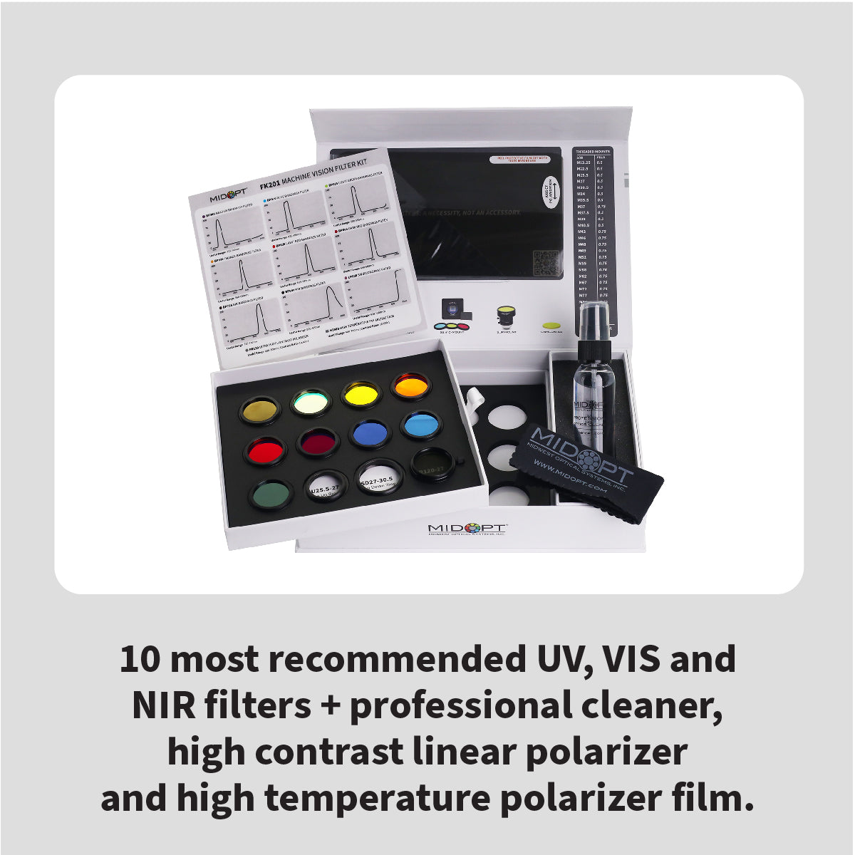
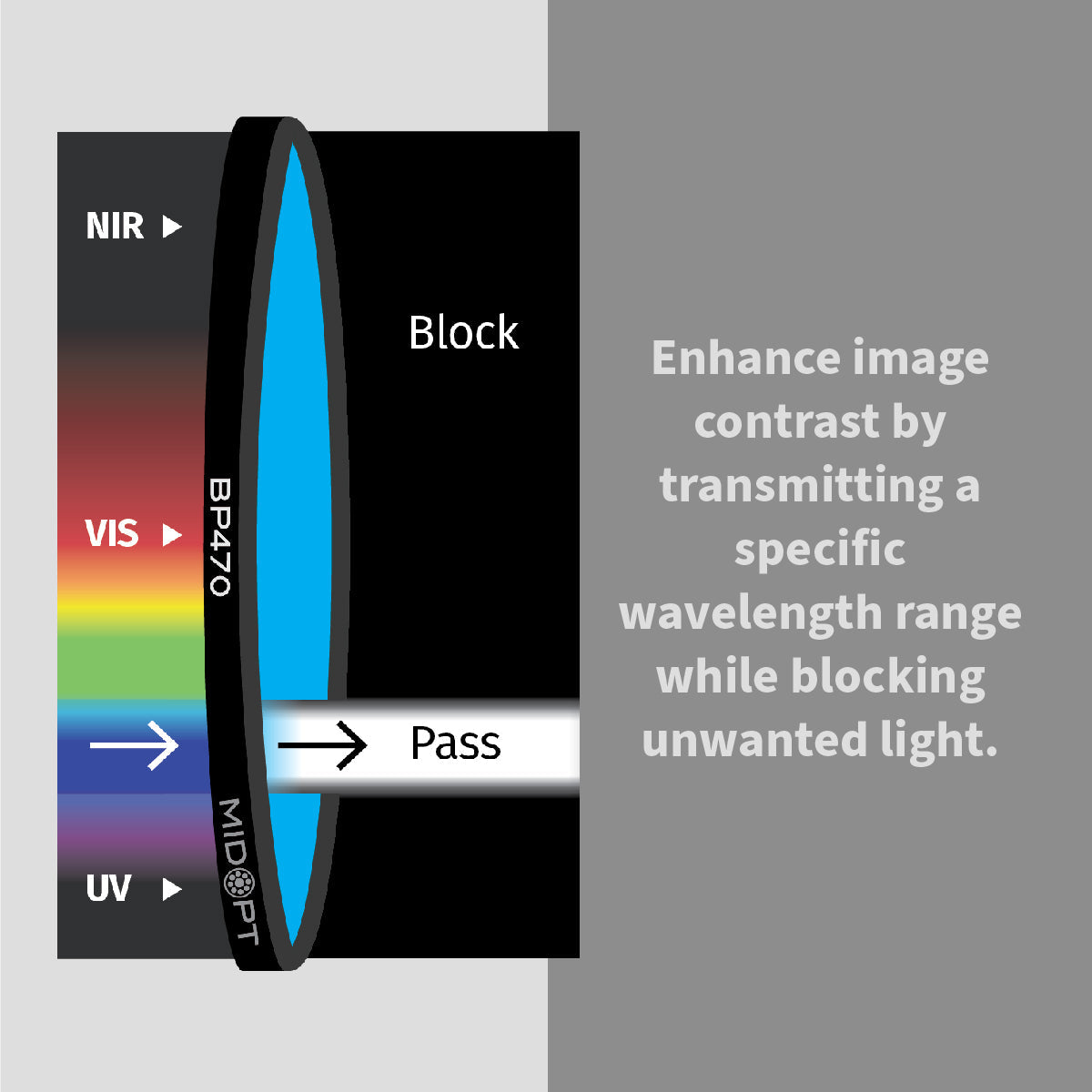
Lighting performance can be improved even further by pairing LED illumination with the appropriate machine vision optical filter.
Matching optical filters help:
- Block ambient factory lighting
- Improve image contrast
- Enhance repeatability
- Increase signal-to-noise ratio
- Reduce unwanted reflections
- Produce cleaner images
Using monochromatic LED illumination with a matching bandpass filter is a proven approach for improving inspection consistency in electronics manufacturing environments.
Selecting the Right Lighting Color
The wavelength of illumination affects how materials appear to the camera.
Different colors may improve visibility of:
- Copper traces
- Green solder masks
- White silkscreen
- Component markings
- Flux residue
- Conformal coatings
- Adhesives
Testing multiple wavelengths often reveals that certain defects become much easier to detect under specific lighting conditions. Choosing the appropriate illumination color is just as important as selecting the lighting geometry.
Building a Complete PCB Inspection System
Successful PCB inspection relies on the integration of every imaging component. A high-performance inspection system typically includes:
- Industrial machine vision camera
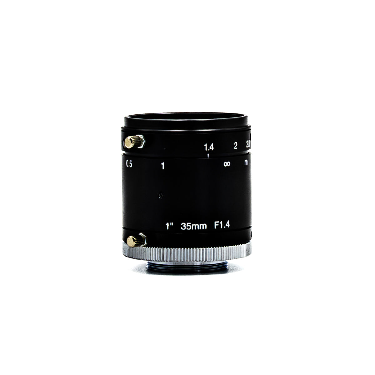
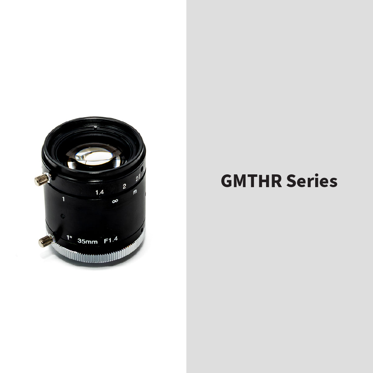
- High-quality machine vision lens
- Optimized LED illumination
- Optical filters
- Image processing software
- Stable mechanical positioning
When these components are selected together, manufacturers achieve higher inspection accuracy, faster production speeds and more reliable quality control.
Improve PCB Inspection with FJW Optical
Glare doesn't have to limit the performance of your inspection system. Properly engineered machine vision lighting dramatically improves image quality by minimizing reflections, increasing contrast, and revealing defects that might otherwise go undetected.
FJW Optical offers a comprehensive selection of machine vision LED lighting for PCB inspection, automated optical inspection (AOI), semiconductor manufacturing, electronics assembly, robotics, industrial automation and precision imaging. Combined with industrial cameras, machine vision lenses, and optical filters, these lighting solutions help manufacturers reduce false rejects, improve defect detection, and achieve more consistent inspection results.
Whether you're designing a new electronics inspection system or optimizing an existing production line, selecting the right lighting strategy is essential for producing clear, repeatable, high-quality images.