
 Find-R-Scopes
 Filters
 Lenses
 Cameras
 Lighting


 Accessories











As electronic devices continue to become smaller, faster, and more sophisticated, manufacturers face increasing pressure to produce flawless products at higher speeds. Printed circuit boards (PCBs), semiconductor devices, batteries, displays, connectors, and electronic assemblies all require precise inspection throughout production to ensure quality and reliability.
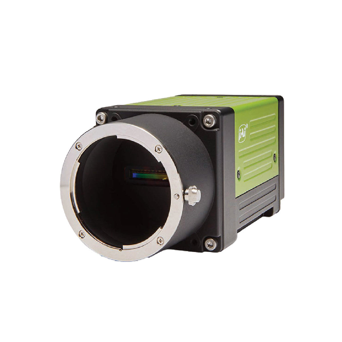
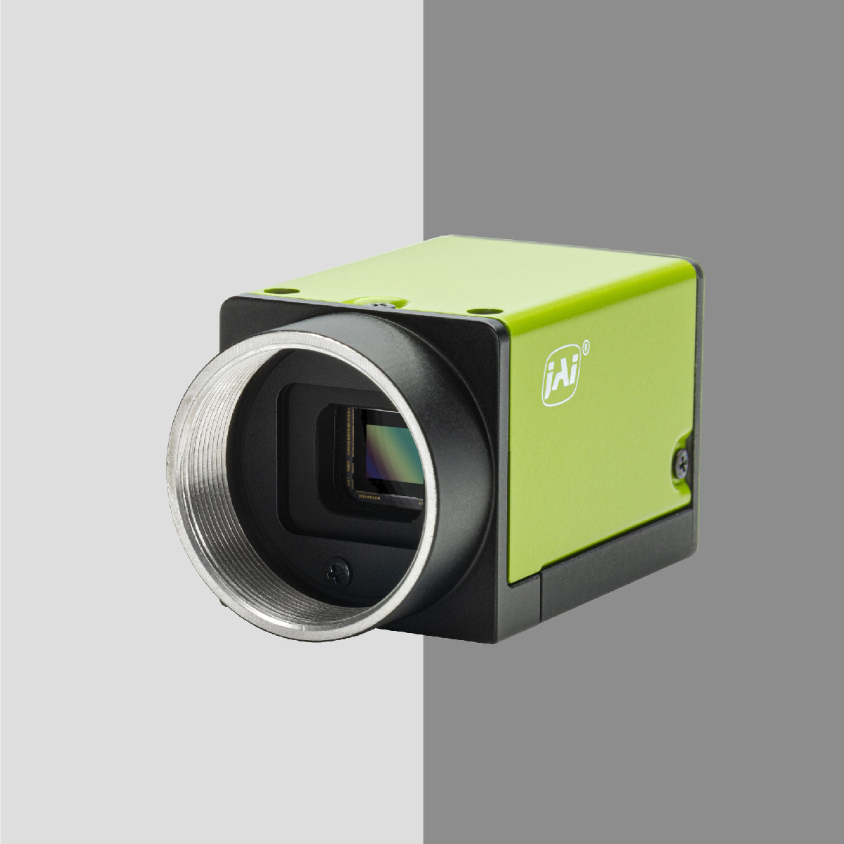
High-resolution machine vision cameras have become a critical component of modern electronics manufacturing, enabling automated inspection systems to detect microscopic defects, verify assembly accuracy and improve production efficiency.
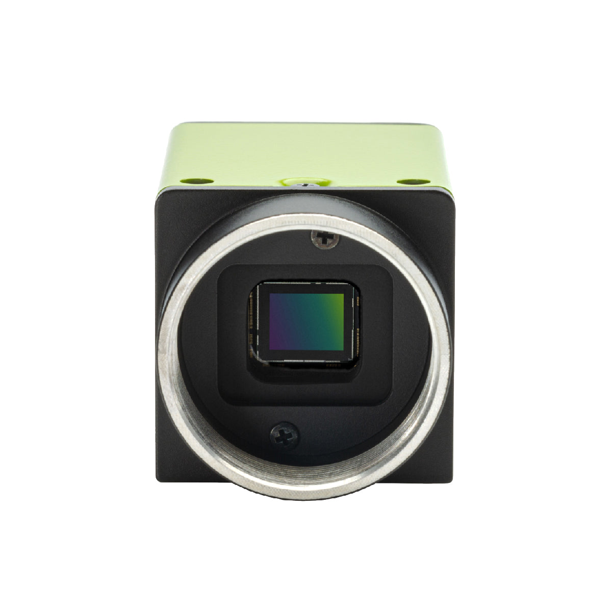
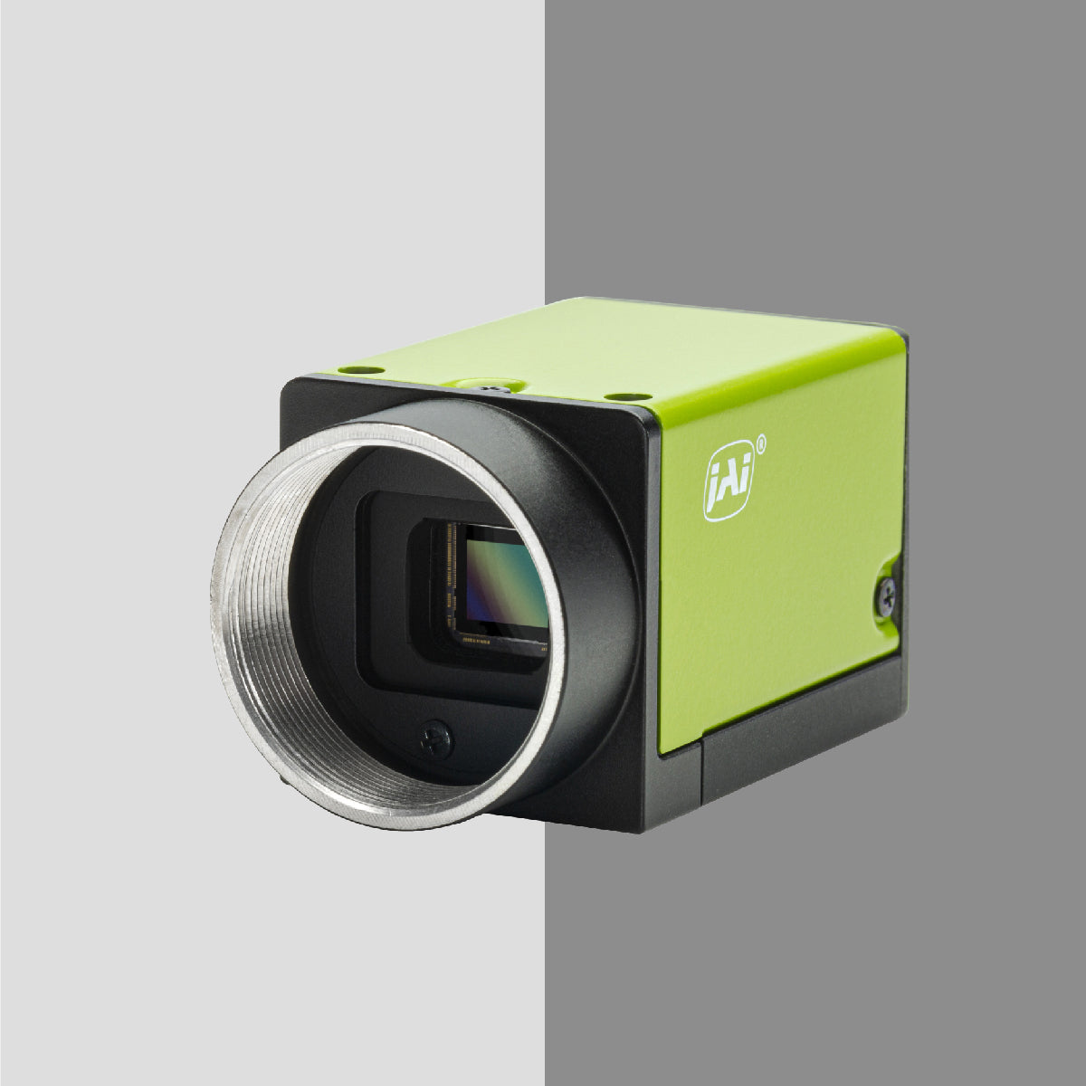
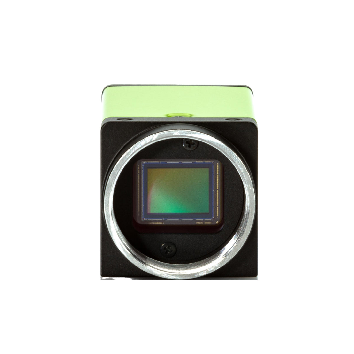
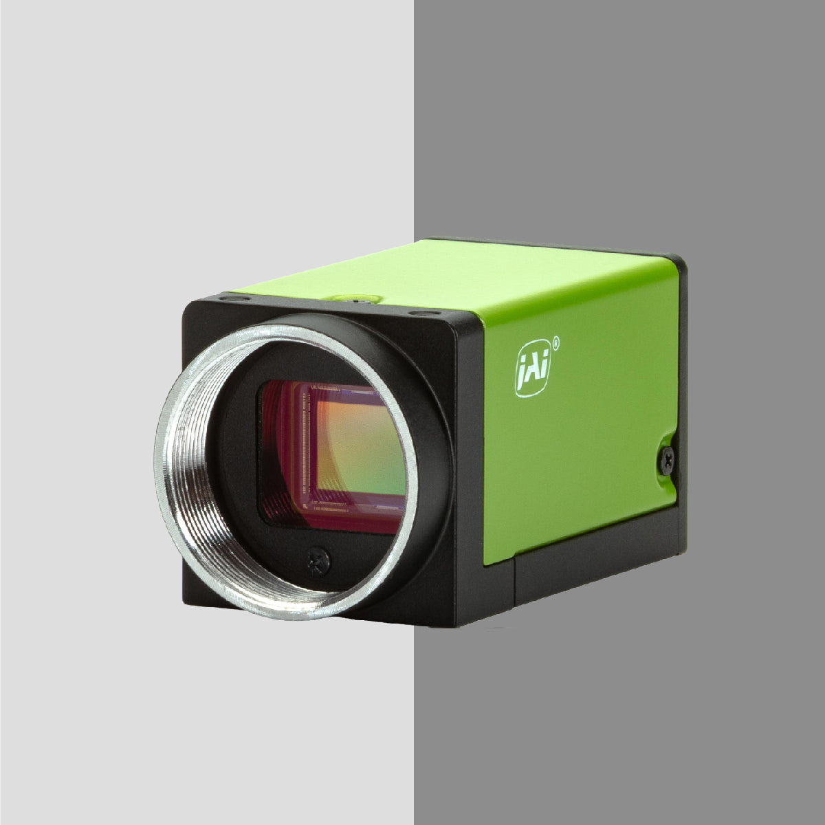
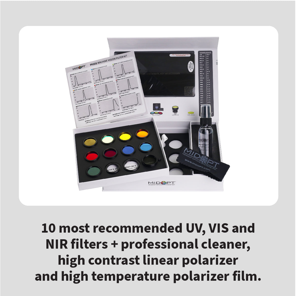
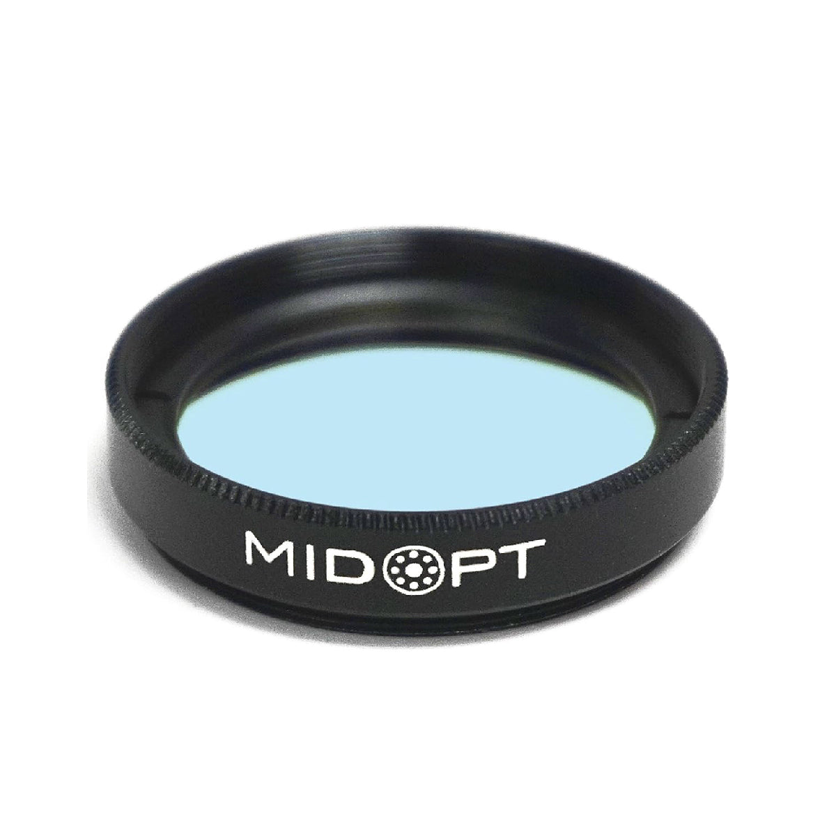
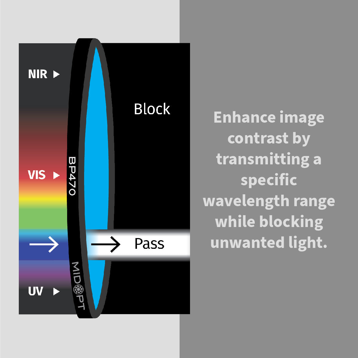
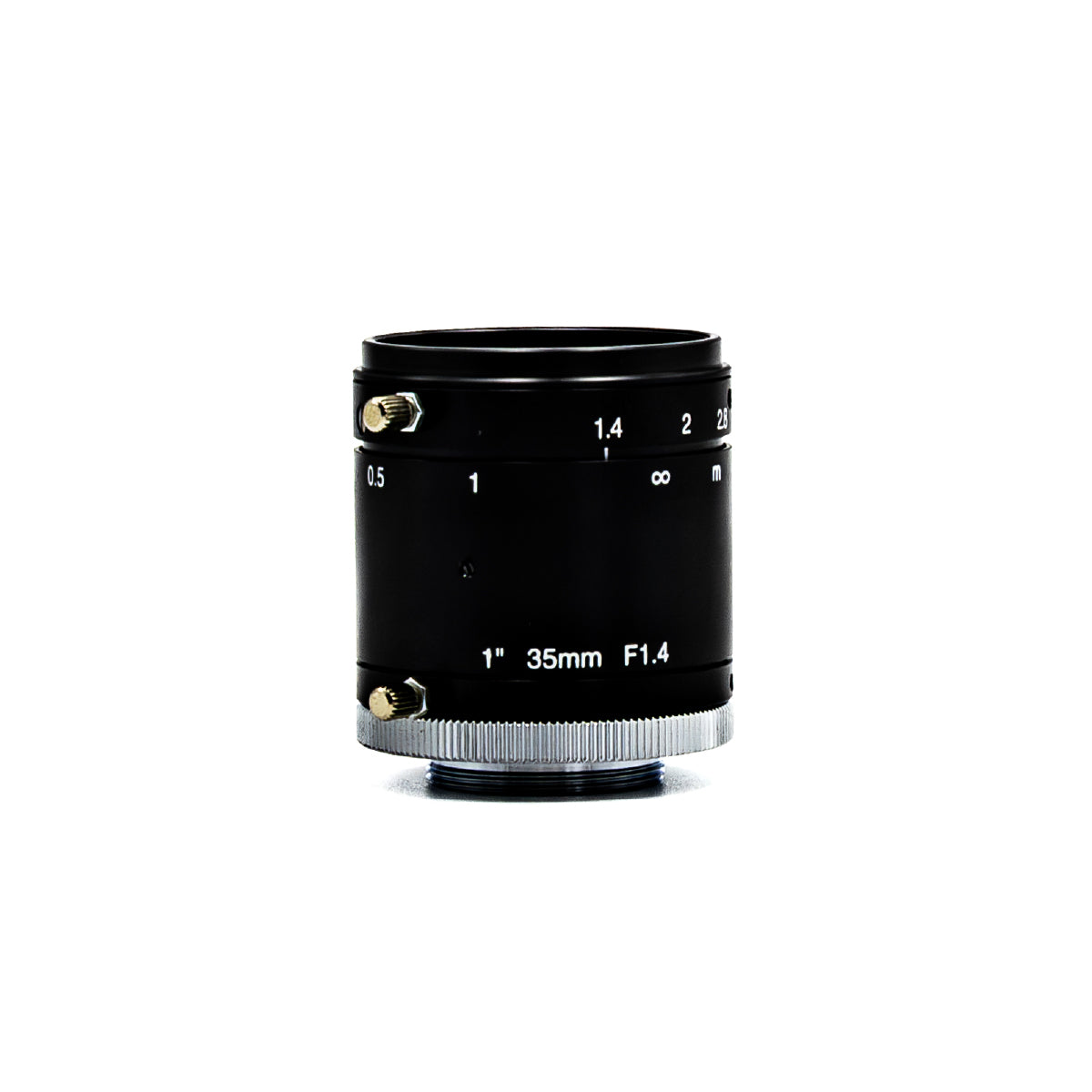
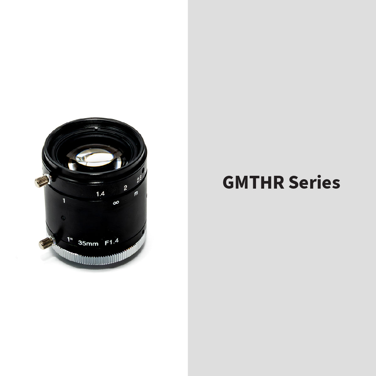
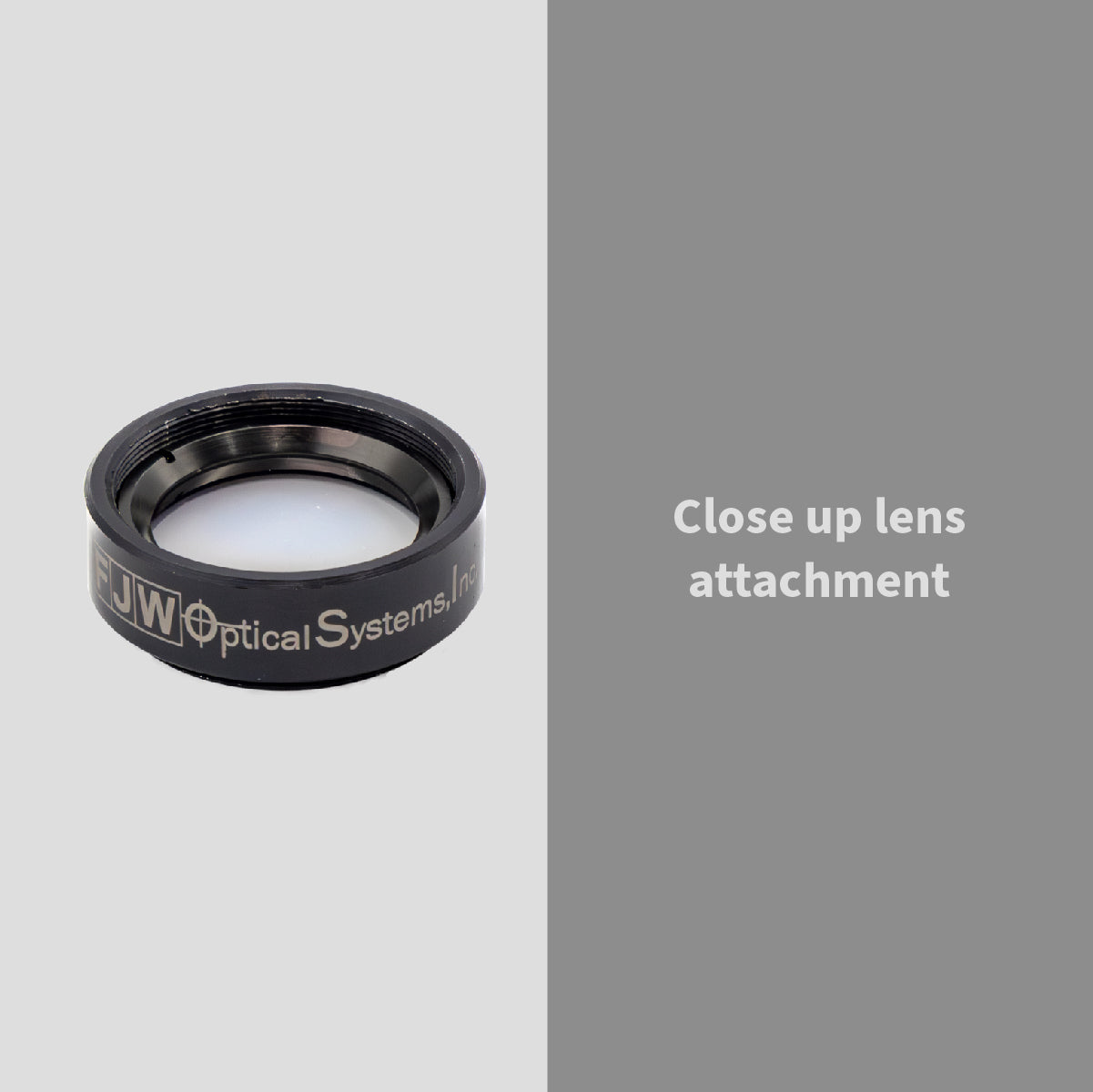
When paired with the proper lenses, lighting and optical filters, today's industrial cameras deliver the image quality needed for demanding electronics inspection applications.
Why Resolution Matters
Electronics manufacturing often involves inspecting features measured in microns. Fine solder joints, miniature surface-mount devices (SMDs), microvias, traces, bond wires and printed markings require exceptional image detail.
Higher-resolution cameras provide:
- Greater measurement accuracy
- Improved defect detection
- Better edge definition
- Higher OCR and barcode reading performance
- More reliable automated inspection
- Increased flexibility for inspecting multiple components within a single image
Instead of adding additional cameras, manufacturers can frequently inspect larger fields of view while maintaining sufficient pixel resolution for accurate measurements.
Common Electronics Inspection Applications
High-resolution machine vision cameras are used throughout electronics manufacturing for:
- Printed circuit board (PCB) inspection
- Automated optical inspection (AOI)
- Surface-mount technology (SMT) verification
- Solder paste inspection (SPI)
- Component placement verification
- Semiconductor inspection
- Wafer inspection
- Battery manufacturing
- Connector inspection
- Display panel inspection
- Flexible circuit inspection
- Laser marking verification
- OCR and barcode reading
- Data Matrix code verification
These inspections help identify defects before products reach final assembly or customers.
Detecting Small Defects with Greater Accuracy
Electronics manufacturers inspect for numerous defects that may be invisible to the human eye.
Examples include:
- Missing components
- Misaligned components
- Lifted leads
- Tombstoned resistors
- Solder bridges
- Cold solder joints
- Cracked solder
- Surface contamination
- Damaged traces
- Scratches
- Micro-cracks
- Foreign particles
High-resolution sensors capture the fine details needed for machine vision software to distinguish acceptable assemblies from defective products.
High-Speed Imaging for Modern Production Lines
Today's production lines operate at extremely high throughput, requiring cameras capable of maintaining image quality while capturing images at high frame rates. Modern industrial cameras combine:
- High-resolution sensors
- Fast image acquisition
- Low image noise
- Excellent dynamic range
- Global shutter technology
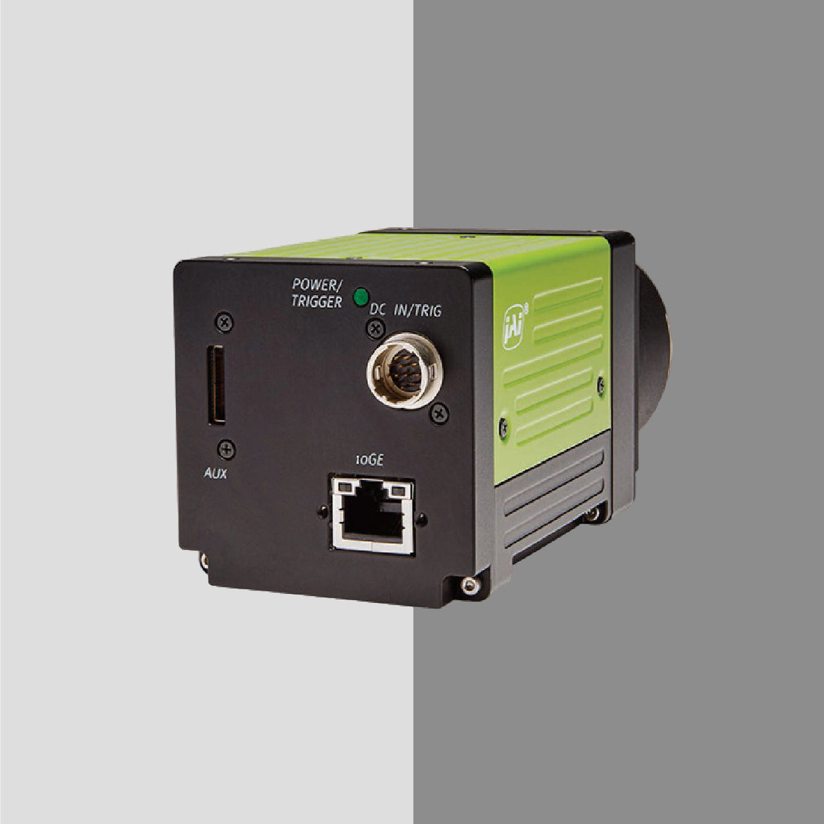
- High-speed data interfaces
This allows manufacturers to inspect every product without slowing production. Fast imaging also reduces motion blur, ensuring sharp images even on rapidly moving conveyor systems.
Global Shutter vs. Rolling Shutter
For many electronics inspection applications, global shutter cameras provide significant advantages. A global shutter exposes every pixel simultaneously, eliminating image distortion caused by object movement.
Benefits include:
- Accurate dimensional measurements
- Reduced motion artifacts
- Reliable defect detection
- Improved inspection consistency
- Better performance on fast-moving production lines
Rolling shutter cameras may be suitable for slower inspections, but high-speed electronics manufacturing often benefits from global shutter imaging.
Color or Monochrome?
Both color and monochrome cameras play important roles in electronics inspection.
Monochrome Cameras
Monochrome sensors generally provide:
- Higher sensitivity
- Better contrast
- Increased resolution
- Improved performance with monochromatic LED lighting
- Superior compatibility with optical filters
These cameras are commonly used for dimensional measurements, solder inspection, and edge detection.
Color Cameras
Color imaging is beneficial for inspections involving:
- Wire color verification
- Component identification
- Label inspection
- PCB solder mask verification
- Color-coded connectors
- Assembly validation
Choosing the correct sensor depends on the inspection objective rather than assuming one technology is universally better.
Large Sensors Increase Productivity
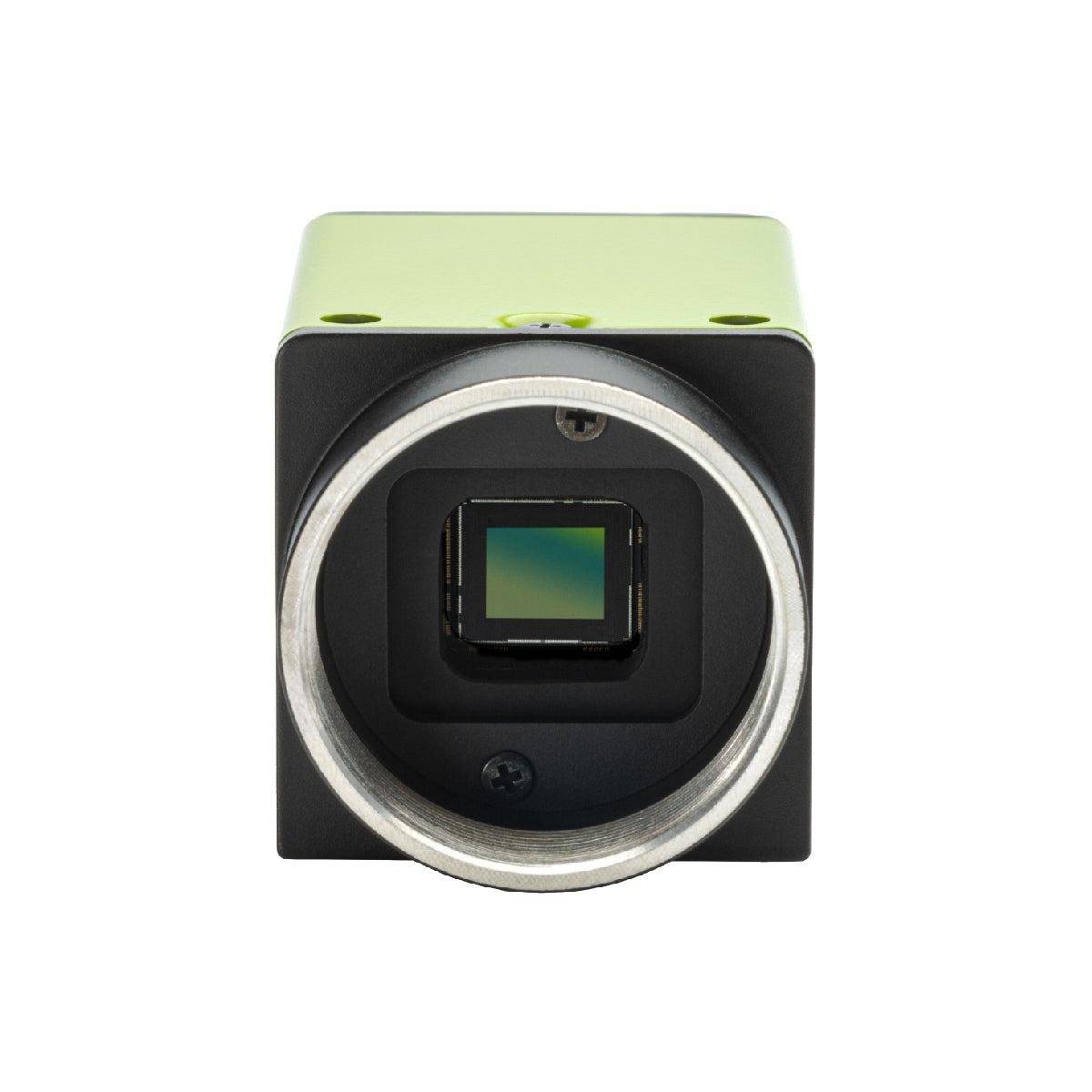
Modern high-resolution cameras often feature larger image sensors that capture wider fields of view while maintaining excellent detail.
Advantages include:
- Fewer cameras required
- Reduced system complexity
- Lower integration costs
- Faster inspection cycles
- Better inspection coverage
- Simplified calibration
This approach is particularly valuable for inspecting large printed circuit boards or multiple assemblies simultaneously.
Excellent Dynamic Range Improves Inspection
Electronic assemblies frequently combine bright reflective metals with darker plastics and matte surfaces. Cameras with high dynamic range capture detail across both bright and dark regions without losing critical inspection information.
Benefits include:
- Better solder joint visibility
- Improved copper trace inspection
- Reduced overexposure
- Greater image consistency
- Enhanced defect detection
Dynamic range becomes especially important when inspecting highly reflective electronic components.
Machine Vision Cameras for Semiconductor Manufacturing
Semiconductor production requires some of the highest imaging performance available.
Applications include:
- Wafer inspection
- Die inspection
- Chip alignment
- Bond wire inspection
- Package inspection
- Surface defect detection
- Lithography verification
High-resolution industrial cameras help manufacturers detect microscopic imperfections before packaging and final assembly.
AI and High-Resolution Imaging
Artificial intelligence continues to transform electronics manufacturing. AI-powered inspection systems rely on high-quality image data to accurately identify defects and classify products. Higher-resolution images provide AI algorithms with:
- More inspection detail
- Better feature extraction
- Increased classification accuracy
- Improved anomaly detection
- Reduced false positives
- Higher confidence levels
The better the image entering the inspection software, the more reliable the AI-driven decision-making process.
Choosing the Right Machine Vision Camera
Selecting the ideal industrial camera involves evaluating several factors:
- Sensor resolution
- Pixel size
- Frame rate
- Sensor size
- Global or rolling shutter
- Monochrome or color imaging
- Dynamic range
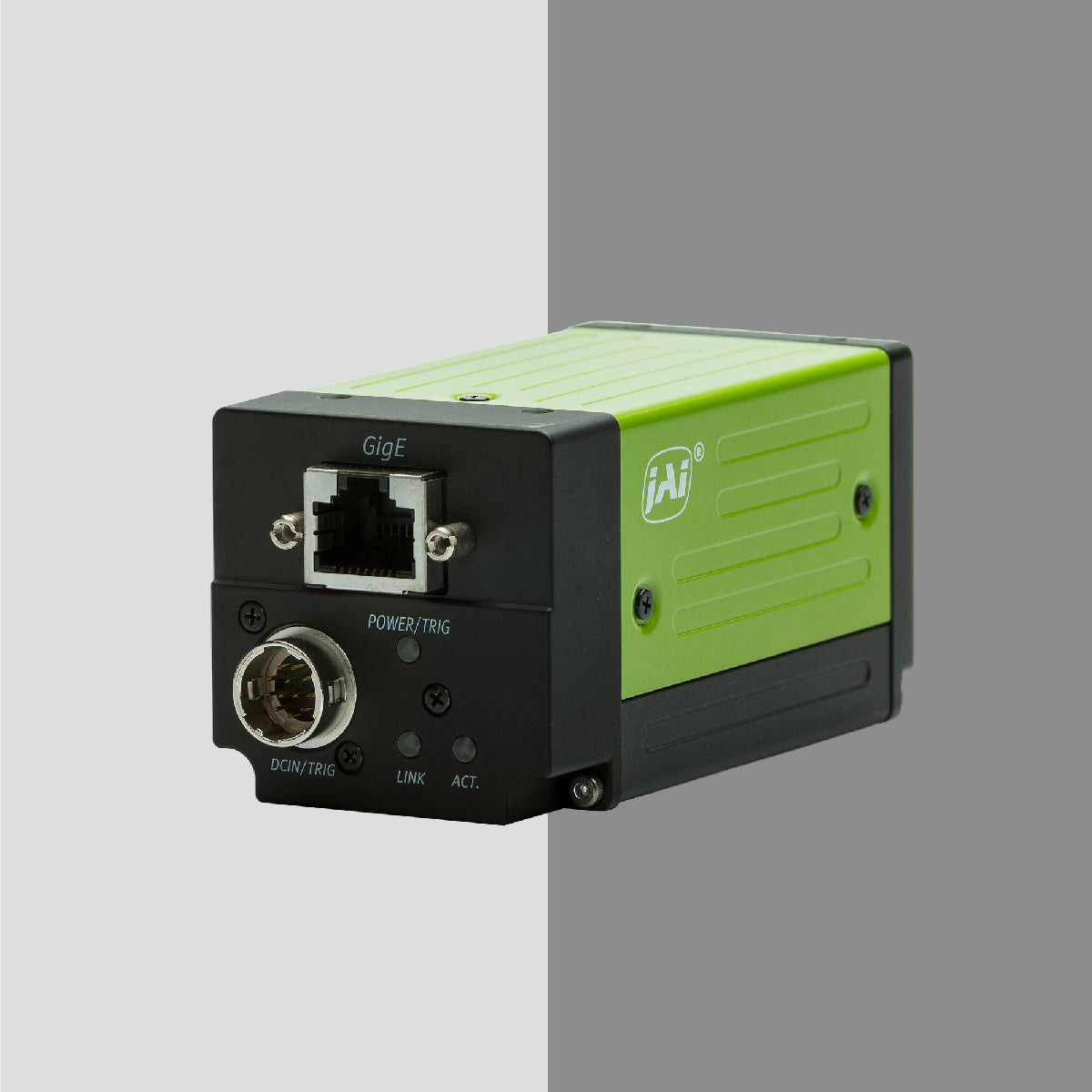
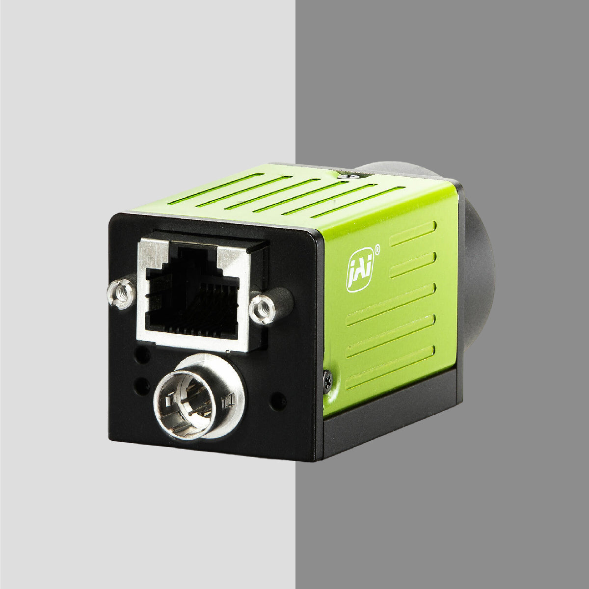
- Interface (GigE Vision®, USB3 Vision®, CoaXPress®, Camera Link®, or 10GigE)
- Working distance
- Lens compatibility
- Lighting conditions
The camera should be selected as part of a complete imaging system that includes appropriate optics, illumination, and optical filters to achieve the best inspection results.
Improve Electronics Inspection with FJW Optical
Reliable electronics manufacturing begins with reliable imaging. High-resolution machine vision cameras provide the precision needed to inspect increasingly complex electronic assemblies while supporting faster production speeds and higher quality standards.
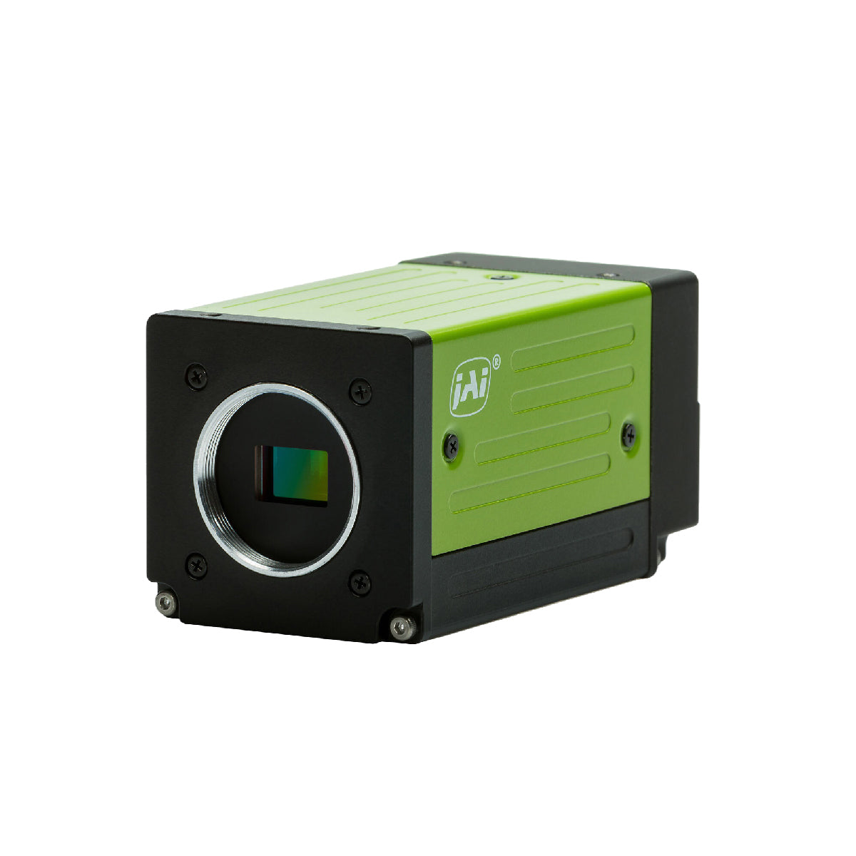
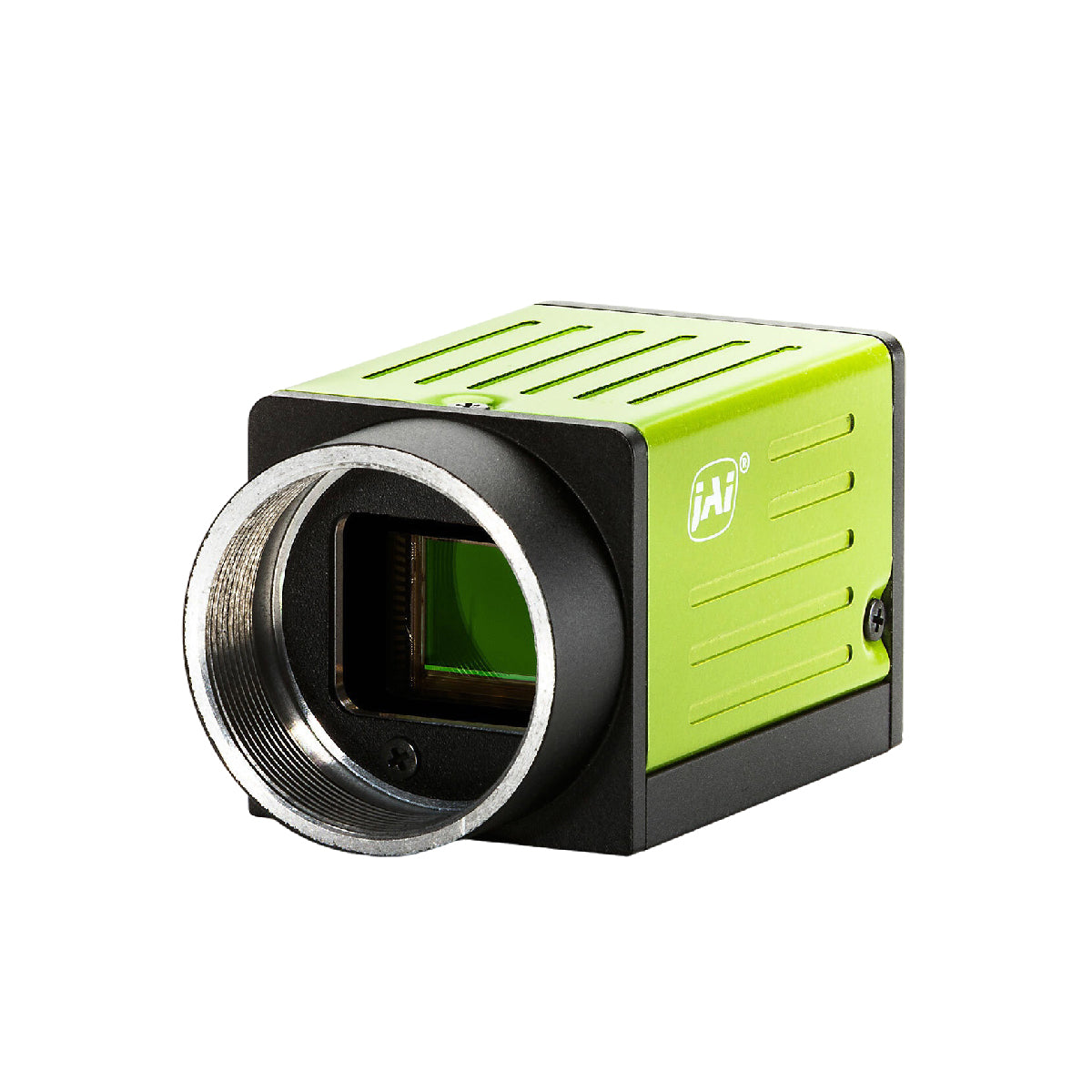
FJW Optical offers a broad selection of industrial machine vision cameras for PCB inspection, automated optical inspection (AOI), semiconductor manufacturing, electronics assembly, battery inspection, display manufacturing, robotics and precision industrial imaging. Combined with high-performance lenses, lighting, and optical filters, these camera solutions help manufacturers improve defect detection, increase throughput, and reduce costly production errors.
Whether you're building a new inspection system or upgrading an existing production line, selecting the right high-resolution camera is a critical step toward achieving consistent, accurate, and efficient electronics inspection.